


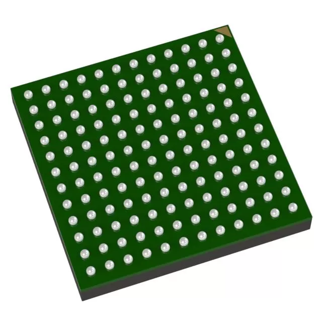

AD8564ARZ
Brand: Analog Devices
Analog Devices AD8564ARZ is a analog & mixed-signal component designed for Instrumentation and related applications. In stock at Superb Automation — request a quote for competitive pricing and fast delivery.
Product Specifications
AD8564ARZ
Analog Devices — Analog & Mixed-Signal ICs
Product Overview
The AD8564ARZ from Analog Devices is a high-performance analog / mixed-signal IC providing precision signal acquisition, conversion, and conditioning. Analog Devices (ADI) is a world leader in high-performance analog, mixed-signal, and DSP ICs for instrumentation, healthcare, automotive, and communications.
Superb Automation partners with leading brands including Qorvo, TI, ADI, XILINX, NVIDIA, Intel, ST, MACOM, Renesas, and Coilcraft to provide complete BOM and supply-chain solutions.
Key Features
- High-resolution data conversion with excellent SNR and THD
- Wide dynamic range and high linearity across operating conditions
- Integrated voltage reference with low temperature drift
- Flexible digital interface — SPI, I2C, or parallel options
- Industrial/automotive temperature range with guaranteed specs
- Low power consumption with power-down modes
Key Specifications
| Resolution | bits |
| Channels | — |
| Sample Rate | kSPS |
| Interface | — |
| Supply Voltage | V |
| Operating Temp | °C |
| Package | — |
| INL | LSB |
| SNR | dB |
| THD | dB |
Applications
Precision Instrumentation
Industrial Process Control
Medical Imaging & Diagnostics
Automotive Sensor Interfaces
Communications Infrastructure
Test & Measurement
Request Quote — In Stock, 100% New & Original, Full Warranty
AD8564ARZ: quad 7 nanosecond comparator on a single 5 volt supply
The AD8564ARZ puts four independent comparators in a 16-lead package with a 6.75 ns typical propagation delay, separate analog and digital supply pins, and TTL and CMOS compatible outputs. It is a timing part, not a precision part: the input offset is millivolts and the bias current is microamps, so the source impedance decides whether the offset or the bias term wins.
Published values
| Parameter | Value |
|---|---|
| Propagation delay | 6.75 ns typical, 9.8 ns maximum on a 200 mV step |
| Rise and fall delay skew | 0.5 ns typical, 2.0 ns maximum |
| Input offset voltage | 2.3 mV typical, 7 mV maximum |
| Offset drift | 4 uV/C typical |
| Input bias current | plus or minus 4 uA at 0 V common mode |
| Input offset current | plus or minus 3 uA |
| Input common mode range | 0 V to 2.75 V on a 5 V single supply |
| CMRR | 65 dB minimum, 85 dB typical |
| PSRR | 80 dB analog, 50 dB minimum on the digital rail |
| Analog supply current | 10.5 mA typical, 14.0 mA maximum |
| Digital supply current | 6.0 mA typical, 7.0 mA maximum |
| Outputs | TTL and CMOS compatible, separate output supply pin |
Microamp bias current meets a millivolt offset
Four microamps into a 1 kOhm source is 4 mV, which is the same size as the 7 mV maximum offset, so a resistive divider driving the input already doubles the error. Into 10 kOhm it is 40 mV and the offset no longer matters at all. This is why the part is used behind a low impedance buffer or on a 50 Ohm transmission line, and why a comparator with a picoamp input belongs in a high impedance socket.
The input only reaches 2.75 V on a 5 V rail
The common mode range stops 2.25 V below the positive rail, so a threshold set at 4 V on a 5 V system will not work. Two ways out: run the analog section from a higher rail, since the analog pins tolerate more than the digital ones, or attenuate the signal so the crossing point sits under 2.75 V. Both change the resolution of the comparison and should be decided before the divider is fixed.
What 21 milliamps buys
Four comparators draw 10.5 mA on the analog rail and 6 mA on the digital rail, so a little over 20 mA with the output currents added. That is the price of a 7 ns edge, and it is fine on a mains powered board and wrong on a battery one. The same socket with a 100 ns comparator costs a tenth of the current.
Skew matters more than absolute delay
Absolute delay of 6.75 ns shifts all four channels equally and a digital system can absorb it. The differential delay of 0.5 ns typical, 2 ns maximum, is what distorts a timing relationship between channels, so a four channel zero crossing detector should be specified on skew rather than on propagation delay. Two nanoseconds at a 20 MHz sampling clock is one twentieth of a period, which is where a multiphase measurement starts to show phase error.
When an order code in this family cannot be found, the amplifier cross reference lists what else does the same job, the ADC and DAC cross reference covers what to check before a part is dropped into an existing board, and component lead time solutions is the route we take on a live shortage.
Two questions buyers ask
Can the outputs drive a 5 V CMOS logic input directly? Yes, the outputs are CMOS and TTL compatible and the output stage has its own supply pin, so the digital rail can be set independently of the analog rail within the ratings.
Is a hysteresis resistor needed? For a slow moving input, yes. Seven nanoseconds of propagation with no internal hysteresis means a noisy signal near the threshold produces a burst of edges, so add positive feedback sized for the noise amplitude.