

RO4350B and RO4003C are the two laminates most RF boards are specified on, and they are close enough that the choice is usually made by habit rather than by calculation. Both are hydrocarbon and ceramic filled, both are processed like FR-4, and both cover the same frequency range. The difference is a lower dielectric constant and a lower loss tangent on RO4003C, paid for with a higher price and a more demanding drilling window.
This page puts the two side by side on the numbers that actually decide a stack-up: Dk, Df, thickness availability, CTE, copper peel strength, and what each one does to a 50 ohm line at 10 GHz and at 24 GHz.
The headline numbers
| Property | RO4350B | RO4003C | Why it matters |
|---|---|---|---|
| Dk at 10 GHz | 3.48 ±0.05 | 3.38 ±0.05 | Line width for a given impedance |
| Df at 10 GHz | 0.0037 | 0.0027 | Insertion loss per unit length |
| Tg (DSC) | >280 °C | >280 °C | Thermal cycles, lead-free assembly |
| CTE, Z axis | 32 ppm/°C | 46 ppm/°C | PTH barrel stress through holes |
| Dk tolerance over frequency | Stable to 10 GHz, drifts above | Stable to 10 GHz, drifts above | Wideband designs |
| Standard thicknesses | 0.004" to 0.060" | 0.008" to 0.060" | Thin inner layers for stripline |
The 0.1 difference in Dk looks small. On a 0.010" thick microstrip it moves the 50 ohm line width by roughly 5 to 8 percent, which is the difference between a design that tunes in on the first pass and one that needs a second iteration. If the board has already been laid out on one material, switching to the other without re-running the impedance calculation will shift every RF trace on the board.
What the loss difference really costs
At 10 GHz, the difference between 0.0037 and 0.0027 in Df is about 0.2 dB per inch of 50 ohm microstrip on 0.010" material. On a 2 inch trace that is 0.4 dB. On a receiver front end with a 3 dB noise figure budget, 0.4 dB of extra loss in front of the LNA is 0.4 dB straight onto the noise figure, and it cannot be recovered downstream.
At 24 GHz the gap widens: roughly 0.5 dB per inch. At 40 GHz it is close to 0.8 dB per inch, and at that point RO4003C stops being optional for anything with more than a few inches of trace.
For a short, low-loss board such as a filter or a coupler under 1 inch of RF path, the difference is a few tenths of a dB. Paying 30 to 40 percent more for RO4003C in that case buys nothing the customer can measure.
Where RO4350B is the better choice
Mixed RF and digital boards. RO4350B behaves like FR-4 in lamination and drilling, and it tolerates a wider drilling window. When an RF front end shares a board with a microcontroller, an FPGA and a power supply, the simpler process usually wins over the last 0.2 dB per inch.
Thin inner layers for stripline. RO4350B is available down to 0.004", which makes a 0.030" stripline stack practical with 0.010" cores and 0.005" prepreg. RO4003C starts at 0.008", so a thin stripline build needs a different construction.
Larger panels and higher layer counts. The lower Z-axis CTE of RO4350B (32 versus 46 ppm/°C) is easier on plated through holes in thick, high-layer-count boards, and it reduces the risk of barrel cracking after multiple reflows.
Cost-sensitive consumer and industrial RF. Wi-Fi front ends, IoT radios, 2.4 and 5 GHz modules and antenna boards rarely need Df below 0.003.
Where RO4003C earns its price
Anything above 20 GHz with real trace length. Radar front ends, SATCOM up and down converters, 24 and 60 GHz sensors, and test equipment front ends. The insertion loss saved per inch is the entire reason the material exists.
Antenna arrays with long corporate feeds. A 16 element array feed network can carry 6 to 10 inches of trace before it reaches the radiators. At 10 GHz that is 1.2 to 2 dB of loss on RO4350B against 0.8 to 1.3 dB on RO4003C, and the difference shows up directly in EIRP and in receive sensitivity.
Low phase drift over temperature. The lower Dk and the tighter Dk tolerance of RO4003C give a more predictable electrical length, which matters for phase-matched feeds and for delay lines in phased arrays.
Processing differences that bite in production
Drilling. Both materials are filled composites, so both drill more like FR-4 than like PTFE. RO4003C is the softer of the two and is more prone to smear at the barrel wall if the drill parameters are pushed. A dedicated drill recipe, with lower feed per revolution and a proper desmear, is standard practice for both, and it should be frozen before the first production lot rather than tuned during it.
Lamination. Neither material needs the low-flow, high-temperature cycle that pure PTFE requires. Standard FR-4 lamination with the supplier's recommended prepreg works, but the press cycle has to follow the laminate datasheet rather than the shop's default FR-4 recipe, especially for thicker builds.
Copper foil. Standard and reverse-treated copper both work. For loss-critical designs above 20 GHz, the copper roughness becomes a larger contributor than the laminate itself, and an HVLP foil is worth more than the step from RO4350B to RO4003C.
Surface finish. ENIG is the default. For low-loss RF, ENEPIG or immersion gold over nickel adds loss at the nickel layer, and bare copper with an organic solderability preservative is not reliable enough for multiple assembly passes. The finish should be selected with the loss budget, not after it.
How to decide in one pass
Start from the loss budget, not from the material table. Add up the allowed insertion loss for the RF path, subtract connector and component losses, and divide what is left by the trace length. That gives a loss per inch figure. Compare it against the two materials at the operating frequency, and pick the cheapest one that fits with margin.
Then check the mechanical side: available thickness for the stack-up, layer count, panel size, and whether the shop has processed the material before. A material that fits the electrical budget but forces a new drill recipe and a new press cycle carries a hidden cost in yield that is usually larger than the laminate price difference.
If the design is a one-off prototype, the material price is noise and the electrical margin should decide. If it is a production program of thousands of boards a year, the laminate cost, the yield and the second-source availability all matter, and the answer is often RO4350B with a tighter stack-up rather than RO4003C with a comfortable one.
Mixing the two on one board
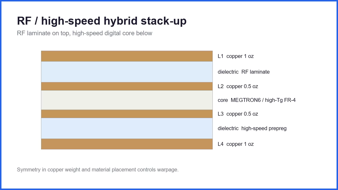
It is common to put RO4003C on the RF layers and RO4350B or FR-4 on the digital and power layers. This works, and it is cheaper than an all-RO4003C build, but the hybrid stack has to be designed as a hybrid from the start: the layer thicknesses change, the prepreg flow changes, and the impedance targets on the RF layers must be recalculated against the actual build rather than carried over from a single-material design.
The failure mode to watch is warpage. Two materials with different CTE laminated into one symmetrical build will bow if the copper balance is uneven, and a bowed RF board does not sit flat against a heat sink or a housing. Symmetry in copper and in material placement, checked at the stack-up stage, is cheaper than fixing it at assembly.
Summary
RO4350B is the workhorse: easier to process, thinner cores available, lower Z-axis CTE, and enough performance for most RF and mixed-signal boards below 20 GHz. RO4003C is the loss-driven choice: about 0.2 dB per inch better at 10 GHz, growing to 0.8 dB per inch at 40 GHz, at a price premium and with a tighter process window.
Choose by the loss budget and by trace length, then confirm the mechanical fit. Do not choose by habit, and do not switch one for the other on an existing layout without re-running the impedance calculation.
Related reading
- RO3003 vs RO4350B for Antenna and Array Boards
- MEGTRON6 vs MEGTRON7: When the Extra Loss Budget Is Worth It
- MEGTRON vs Rogers: Two Different Problems, Not Two Brands
- Ceramic-Filled PTFE vs Pure PTFE: Which RF Substrate?
- How Dk and Df Are Measured, and Why Datasheets Disagree
- RF PCB manufacturing
- RF and microwave PCBA





