

Two laminate datasheets can quote the same Df and the boards will not lose the same amount of signal. They can quote the same Dk and the impedance will not come out the same. The reason is that Dk and Df are not properties of a material in the abstract: they are results of a measurement method, at a frequency, on a test structure, and the number you design with is a fourth thing again, the process Dk that comes out of the fab.
This page explains what the common test methods actually measure, why the numbers differ, and how to compare two datasheets without being misled.
The four numbers behind one "Dk"
Material Dk. The value from the supplier's characterisation, usually a clamped stripline or a resonator at a stated frequency. It is a property of the dielectric, measured in a structure that is not your board.
Effective Dk. What a microstrip line actually sees, including the air above the trace and the fields that fringe into it. For the same material, effective Dk is always lower than material Dk, and the difference depends on line width and substrate thickness.
Design Dk. The number a fabricator uses in the field solver so that the finished impedance matches the target. It is calibrated against measured test coupons and is usually a little different from the material Dk, because it absorbs etch factor, prepreg flow and plating thickness.
Process Dk. What the board actually has after lamination and plating. It drifts lot to lot, which is why impedance tolerance is stated in percent and not in ohms.
Most design arguments happen because one person is quoting number one and another is quoting number three.
How the common methods work
| Method | Standard | Frequency range | What it is good for |
|---|---|---|---|
| Clamped stripline resonator | IPC-TM-650 2.5.5.5 | Roughly 1–12 GHz | Baseline Dk and Df, comparable across suppliers |
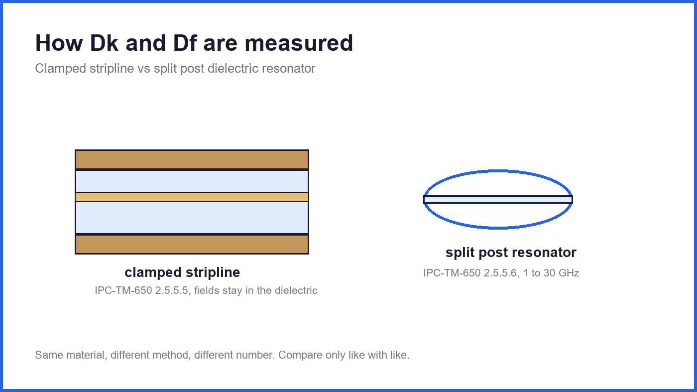
| Split post dielectric resonator (SPDR) | IPC-TM-650 2.5.5.6 | Roughly 1–30 GHz | Fast, small sample, good repeatability |
| Full-sheet resonance | IPC-TM-650 2.5.5.7 | Varies | Large-area uniformity, glass weave effects |
| Microstrip / stripline coupon | Customer or fab method | Design frequency | What the board will actually do |
| Free-space / Fabry–Perot | Millimetre-wave methods | 30 GHz and above | mmWave characterisation |
A clamped stripline measurement puts the sample between two ground planes with a resonator pattern etched on it. Because the fields are almost entirely inside the dielectric, the result is close to the true material Dk. A microstrip coupon leaves half the field in air, so the effective Dk comes out lower and the loss includes radiation and surface roughness.
Neither is wrong. They answer different questions, and a datasheet that does not state the method and frequency is not a comparable number.
Why Dk changes with frequency
All polymer-based laminates show Dk falling slowly with frequency and Df rising. Over 1 to 10 GHz on a hydrocarbon laminate, Dk typically drops by 1 to 3 percent. On PTFE the change is smaller. On FR-4 it can be larger, and the curve is steeper above 5 GHz.
This matters because a design done with the 1 GHz number and built at 28 GHz will have a lower Dk than assumed, which shifts impedance up and moves every resonant structure up in frequency. For a filter, that is the difference between passing and failing the first article.
For mmWave designs, ask the supplier for the Dk curve, not the single value. Rogers publishes curves for its RF materials; Panasonic publishes tables at several frequencies. If the curve is not available, measure at the design frequency on a coupon.
Why Df is worse than it looks
Df is small, and small numbers are easy to misquote. A datasheet may say 0.002 at 1 GHz and the same material may measure 0.004 at 10 GHz. Both statements are true.
The second trap is that measured insertion loss includes conductor loss. A board with rough copper can show a total loss that looks like a much worse Df, and a designer comparing two materials on measured board loss may attribute the difference to the laminate when it is the foil.
When comparing Df across suppliers, check three things: the frequency, the method, and whether copper roughness was corrected. Without those, a 0.001 difference may be measurement, not material.
The copper roughness correction
At high frequency, current crowds into the surface of the copper, and a rough surface makes the path longer. The correction models (Hammerstad, Huray snowball) convert measured loss into a dielectric-only loss so that materials can be compared fairly.
For the designer, the practical point is simpler: on the same laminate, moving from standard foil to HVLP can reduce insertion loss by 10 to 20 percent at 25 GHz. That is often more than the difference between two adjacent laminate grades. Before paying for the next grade up, check which foil the stack uses.
Glass weave and local Dk
On glass-reinforced materials, the resin and the glass have different Dk. A trace that runs along a glass bundle sees a different effective Dk than one that runs between bundles. On a differential pair, the two traces can see different values, which shows up as skew.
The standard fixes are spread glass, rotated glass, or routing at an angle to the weave. For high-speed digital this is a skew problem; for RF filters it is a centre-frequency problem. Either way it is a material structure issue, not a Dk number issue, and it will not appear in a datasheet.
What to ask a supplier
Four questions turn a datasheet into a design input: what method was used, at what frequency, on what thickness, and what is the tolerance over production lots.
For RF and mmWave work, add: do you have Dk and Df curves up to the design frequency, and what is the Dk tolerance lot to lot. A material with Dk ±0.05 and a flat curve is easier to design with than one with Dk ±0.02 that moves 3 percent across the band.
What a fabricator should give back
A first article should include impedance coupon results per layer, the measured Dk back-calculated from those coupons, and a note on which foil was used. That closes the loop between the datasheet number and the board in the customer's hand.
If the measured impedance is consistently 3 percent high across every layer, the design Dk is wrong, not the process. If it wanders layer to layer, the process is the problem. Distinguishing the two is the whole point of putting coupons on the panel.
Summary
Dk and Df are measurement results, not constants. Compare datasheets only at the same frequency and method, ask for curves above 10 GHz, and treat the design Dk from the fab as the number that actually determines impedance. When a design misses its centre frequency, check the foil and the glass weave before blaming the laminate.
Related reading
- Dk Drift: Why an RF Board Changes With Temperature and Humidity
- PTFE PCB Manufacturing: Process Control From Drill to Lamination
- RO4350B vs RO4003C: Which RF Laminate Should You Specify?
- RO3003 vs RO4350B for Antenna and Array Boards
- MEGTRON6 vs MEGTRON7: When the Extra Loss Budget Is Worth It
- RF PCB manufacturing
- RF and microwave PCBA





