

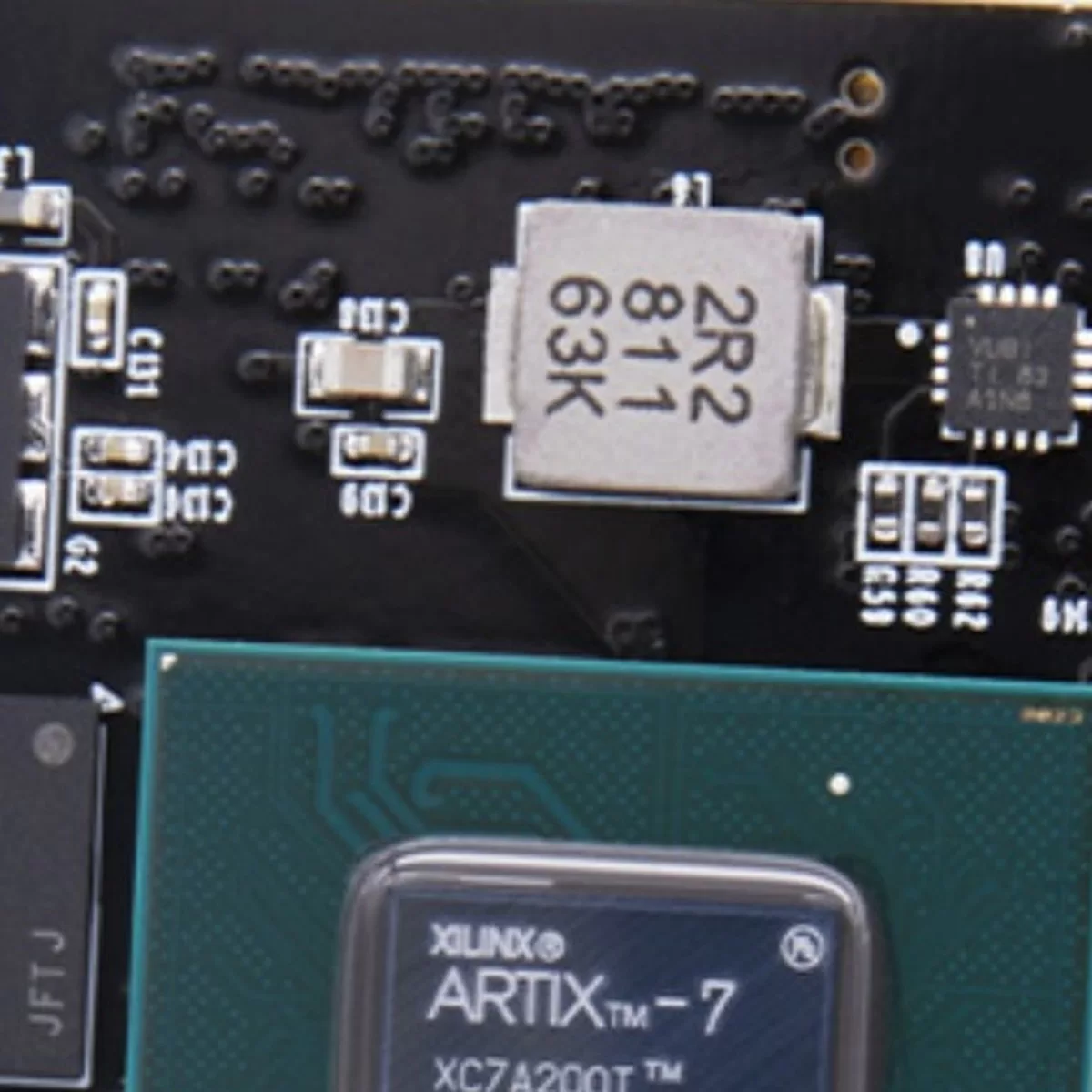
A PTP grandmaster clock is the box that gives a 5G network its sense of time. It takes time from GNSS or a primary reference, holds it steady with an oscillator, and hands it to every radio unit over Ethernet using IEEE 1588 Precision Time Protocol. Without a grandmaster, a TDD radio does not know when to switch from downlink to uplink, and the cell stops working.
Why a radio unit cannot just use its own clock
Every radio unit has a local oscillator, and every local oscillator drifts. In FDD that drift only shifts the carrier slightly. In TDD it moves the switch point between transmit and receive, which puts uplink slots on top of the neighbour cell's downlink slots.
3GPP sets the budget at ±1.5 µs of phase error for basic TDD operation. That sounds generous until you subtract everything between the grandmaster and the antenna: packet delay variation in the transport network, the radio unit's own internal delay, and temperature drift over the day. Most operators run their transport to a much tighter internal target, because the last few hundred nanoseconds are consumed by the radio itself.
Coordinated features are stricter. MIMO coordination, carrier aggregation across sites and O-RAN split architectures all depend on the same time base, and some of them tighten the requirement to a few hundred nanoseconds or better. That is why PTP, not NTP, is used: NTP typically lands in the low milliseconds, three orders of magnitude away from what a TDD radio needs.
What is actually inside a grandmaster board
Four blocks matter, and each one can fail the timing budget on its own.
GNSS receiver. Multi-constellation, multi-band receivers reject multipath better than single-band ones. The receiver has to output more than a position: it has to produce a 1PPS edge and time-of-day that the PTP stack can discipline against.
Oscillator. A TCXO is enough when the GNSS view is clear and outages are short. An OCXO earns its cost when the site has a poor sky view or the operator needs hours of holdover. The number that matters is not the free-running stability, it is the holdover slope: nanoseconds per hour, measured at the temperature the board actually sees.
Timestamping. Hardware timestamping in the PHY is the default for a reason. Software timestamping moves the measurement point into the kernel scheduler, where a busy CPU adds microseconds of jitter that no amount of filtering removes.
Outputs and management. 1PPS, 10 MHz, time-of-day over serial, and a management path for monitoring. These are the signals the test bench will measure, so they need to be accessible and documented.
Where grandmaster boards go wrong in the field
Antenna delay is not calibrated. The cable between the GNSS antenna and the receiver delays the signal by a few nanoseconds per metre. If that value is left at zero, the whole network is offset by a constant that nobody notices until a neighbouring network is compared against it. It is a single configuration number and it is skipped constantly.
Holdover is specified on paper but never tested. A holdover claim measured at 25 °C in still air tells you very little about a cabinet at 60 °C with a fan failure. Holdover has to be measured with the GNSS input removed, at temperature, for the duration the operator actually needs.
The oscillator is placed for layout, not for thermal reasons. An OCXO next to a power converter or a hot FPGA will meet its specification for the first month and then drift as the enclosure heat-soaks. Thermal isolation is a mechanical decision that gets made after the schematic is frozen, which is the wrong order.
Jitter is checked with the wrong instrument. A scope probe on a 1PPS output shows you the edge, not the phase error over 24 hours. Meaningful verification needs a time interval analyser or a phase measurement against a reference, logged over hours.
How these boards are built and tested
Grandmaster boards are mixed-technology assemblies: a GNSS front end with controlled impedance feedlines, a digital section running DDR and Ethernet PHYs, an OCXO with its own thermal and mechanical requirements, and coax or board-to-board connectors that have to survive reflow and mating cycles. That combination is where assembly quality decides whether the timing budget survives production.
At Superb Automation we build these boards to print and support the test plan the design defines. Relevant capability for this board type:
- 01005 and 0201 placement, 0.35 mm pitch QFN and LGA, with X-ray on thermal and ground pads
- Mixed RF and digital assembly on the same panel, with impedance-controlled stack-ups and selective conformal coating
- Connector and OCXO handling on thermally sensitive assemblies, including keep-out and shielding frames
- Functional test fixtures, 1PPS and phase error measurement support, and serial-level traceability to the component lot
The timing design, the PTP stack and the holdover specification belong to the design owner. Our job is to keep the assembled board inside that budget, batch after batch, and to give you the measurement data that proves it.
If you are building a grandmaster, a boundary clock or a timing distribution board, send the Gerber, BOM and test specification. We will come back with a DFM review and a quote.





