

A board that measures perfectly on the bench at 25 °C can fail in the field at 85 °C or at -40 °C, and the reason is usually not a component. It is the laminate: Dk moves with temperature, and on a phase-critical design that movement turns into phase error, frequency shift and, in an array, beam pointing error.
This is the least discussed laminate parameter and the one that costs the most rework in radar, SATCOM and instrumentation programs.
What moves, and by how much
| Parameter | Typical behaviour | Effect on the circuit |
|---|---|---|
| Dk vs temperature (TCDk) | Tens of ppm/°C, sign depends on material | Phase drift, frequency shift |
| Dk vs frequency | Falls 1–3% from 1 to 10 GHz on hydrocarbon; smaller on PTFE | Impedance and resonance shift across band |
| Dk vs moisture | Rises with absorbed water | Frequency shift in humid environments |
| CTE, in-plane | 15–20 ppm/°C for most RF laminates, closer to copper | Board growth, connector alignment |
| Dimensional change through assembly | 0.02–0.05% typical | Array pitch, feed alignment |
The absolute numbers vary by material family and by supplier, and they are small. The reason they matter is that phase is proportional to electrical length, so a long delay line multiplies a small Dk change into a large phase change.
The arithmetic that catches designers
Phase through a line is 360 degrees times electrical length divided by wavelength. A 1 percent change in Dk changes the electrical length by about 0.5 percent, because phase scales with the square root of Dk. On a 10 wavelength line at 10 GHz, that is 18 degrees of phase shift for a 1 percent Dk change.
Now put that in a phased array with a corporate feed and phase shifters calibrated at room temperature. A 18 degree error across the band is a beam pointing error, and in a receive array it shows up as gain loss in the steered direction.
The same arithmetic applies to a filter: a 1 percent Dk change moves the centre frequency by roughly 0.5 percent, which on a 10 GHz filter is 50 MHz. A narrowband filter with a 100 MHz passband has just lost half its margin.
Temperature: the big one
Most RF laminates specify a TCDk in the tens of ppm/°C range. Some are positive, some negative, and in a hybrid stack the two can partly cancel or add, depending on which layer carries the critical line.
Over a 100 °C swing, a TCDk of 50 ppm/°C gives a 0.5 percent Dk change, which is 0.25 percent in electrical length, or about 4.5 degrees per wavelength at the design frequency. On a 5 wavelength delay line that is 22 degrees. On a 20 wavelength line it is 90 degrees.
This is why phase-critical designs ask for the TCDk curve rather than a single number, and why some programs specify a material partly on the flatness of that curve rather than on loss.
Moisture: the slow one
Water has a Dk of about 80. Even a small absorbed fraction raises the effective Dk of the laminate. FR-4 absorbs on the order of 0.1 to 0.2 percent by weight; PTFE absorbs well under 0.02 percent; hydrocarbon materials sit in between.
The practical consequence: a board tuned dry will drift when it sits in a humid equipment room, and it will drift back when it dries out. For outdoor units, this is a seasonal frequency shift that shows up as a service call every summer.
For tight-tolerance RF, specify low-absorption material and, just as importantly, specify the moisture condition under which the factory tunes the board. A board tuned wet and installed dry is out of specification from day one.
Frequency: the one people forget
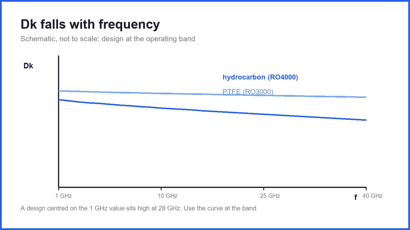
Dk falls with frequency. A design centred using the 1 GHz value will sit high in frequency at 10 GHz and higher still at 28 GHz. On a broadband design this shows as a tilt in the passband; on a narrowband design it shows as a centre-frequency error.
The fix is simple and often skipped: use the Dk curve at the design frequency, and if only one number exists, measure a coupon at the design frequency.
Assembly: the hidden shift
Lamination and reflow cause dimensional change. A 0.03 percent shrink on a 200 mm panel is 60 µm, which on a 5 mm array pitch is enough to move the feed network off the radiator by a visible amount at 77 GHz.
This is why array designs specify the material's dimensional stability through assembly, and why the fab should report the measured shrink per lot. It is also why hybrid stacks with different materials on different layers need a coupon that measures the whole build, not just the RF core.
How to control it
Design: keep the phase-critical line lengths as short as the architecture allows, because error is proportional to length. Where long delays are unavoidable, use a material with a flat TCDk curve.
Stack-up: put the phase-critical lines on one material, not across a hybrid boundary, so the drift is uniform and can be compensated.
Calibration: if the system has phase calibration, calibrate at the temperature the system will run at, or calibrate at two temperatures and interpolate. Room-temperature calibration on a system that runs at 70 °C bakes in the error.
Specification: ask for TCDk, moisture absorption and dimensional stability in the material spec, and ask the fab for coupon data at temperature if the program is phase-critical.
What this means for material choice
For most digital and consumer RF work, none of this matters: the frequency is low, the lines are short and the margins are wide. For radar, SATCOM, phased arrays and instrumentation, it is the difference between a product that holds calibration and one that needs a service visit.
When a program is phase-critical, the laminate decision should be made on three curves: Dk against frequency, Dk against temperature, and absorption. Loss matters, but a low-loss material with poor dimensional stability will still fail the phase requirement.
Related reading
- PTFE PCB Manufacturing: Process Control From Drill to Lamination
- RO4350B vs RO4003C: Which RF Laminate Should You Specify?
- RO3003 vs RO4350B for Antenna and Array Boards
- MEGTRON6 vs MEGTRON7: When the Extra Loss Budget Is Worth It
- MEGTRON vs Rogers: Two Different Problems, Not Two Brands
- RF PCB manufacturing
- RF and microwave PCBA





