

PTFE boards are not hard to build once the process is set up for them. They are hard to build when the shop treats them as expensive FR-4. The failures are consistent and well known: smeared holes, delamination at the dielectric-copper interface, thickness loss in the press, and plated barrels that crack after thermal cycling.
This page is the process checklist we use when qualifying a PTFE build, written in the order the board actually goes through the line.
1. Material receiving and storage
PTFE laminates arrive with a protective film on both sides and a shelf life. Store them flat, in the original packaging, away from direct sunlight and heat. Do not stack heavy panels on thin cores.
Check the datasheet revision against the purchase order. Laminate suppliers revise Dk and process recommendations between revisions, and a stack-up calculated on an older datasheet can be off by enough to miss the impedance target.
2. Inner layer imaging and etch
PTFE is soft and Dimensionally it moves more than FR-4 during the imaging and etch steps. Two controls matter.
Etch compensation. PTFE etches differently from FR-4 because there is no glass to undercut. The etch factor has to be measured for the specific material and line width, not carried over from an FR-4 job.
Handling. Soft cores scratch. Scratches on an inner layer become pits after lamination, and pits under an RF trace change the local Dk. Handle with gloves, keep the film on until the last step, and inspect under the right light.
3. Drilling
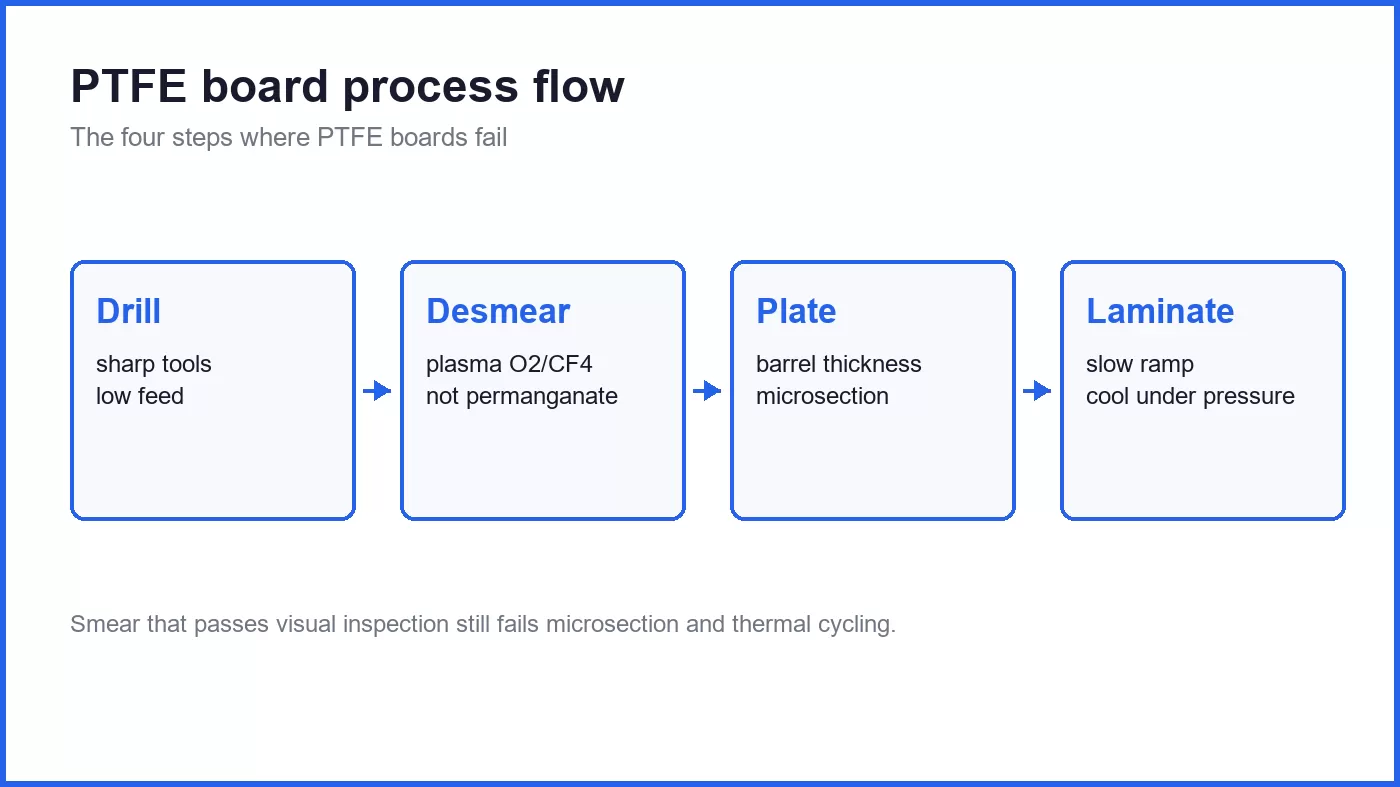
This is where most PTFE failures start. PTFE does not cut cleanly; it smears. The smear is conductive residue that sits on the barrel wall and on the inner-layer pads, and it causes intermittent opens that pass electrical test and fail in the field.
Tooling. Sharp carbide drills, dedicated to the job. Worn tools generate heat, and heat makes PTFE smear.
Parameters. Lower spindle speed and lower feed per revolution than FR-4, with a retract that clears the chip. The exact numbers depend on the material and thickness and must come from the laminate supplier's process guide, not from a generic table.
Entry and exit material. Use proper entry and backing to support the soft dielectric and to prevent burring on the exit side.
Hits per tool. Plan for fewer hits than on FR-4. The cost of a drill bit is trivial compared with a rework lot.
4. Desmear and hole wall preparation
Standard permanganate desmear does not remove PTFE smear effectively. Two methods are used.
Plasma desmear. The standard approach. An oxygen and CF4 plasma attacks the PTFE surface, removes smear and creates the chemical roughness that plating adhesion depends on. Plasma time and gas mix are material-specific.
Sodium naphthalenide. A wet process that etches PTFE chemically. It works, but it is aggressive, it needs careful rinse control, and it is less common in shops that run mixed materials.
Whichever is used, the acceptance criterion is a microsection: no smear on the barrel, no voids at the copper-dielectric interface, and a hole wall that is uniformly prepared. Visual inspection after plating tells you nothing about smear.
5. Lamination
PTFE flows. The press cycle has to be built around that.
Bondply. Use a PTFE-compatible bondply or prepreg specified by the laminate supplier. FR-4 prepreg will not bond properly to PTFE, and the failure shows up as delamination after thermal stress, not at first inspection.
Ramp and pressure. Slower ramp, lower pressure, longer dwell than an FR-4 cycle. High pressure squeezes the dielectric and drops the thickness, which moves the impedance of every layer.
Cooling under pressure. Cool the stack under pressure to below the bondply's softening point before opening the press. Opening early causes warpage and, on thin builds, delamination.
Thickness check. Measure the finished thickness at multiple points on the panel and compare against the stack-up target. A 10 percent thickness error on a 0.010" core is a straightforward impedance miss.
6. Plating and PTH reliability
PTFE's high Z-axis CTE relative to copper puts stress on the plated barrel. Three controls reduce the risk.
Plating thickness. Meet the class requirement on the hole wall, not just at the surface. Thin plating on a soft dielectric is where barrel cracks begin.
Thermal stress test. Run the standard thermal stress or IST test on the first article and on the first production lot. A barrel that survives one reflow can still fail after 100 thermal cycles.
Microsection. Cut the first article, measure plating thickness at the knee and mid-barrel, and check for voids and resin recession. Photograph it and keep it with the lot record.
7. Surface finish
ENIG is the default for RF boards. Two cautions: the nickel layer adds loss at high frequency, and thin or porous gold over nickel will oxidise in storage.
For millimetre wave, ENEPIG or a controlled-thickness immersion gold is preferred, and the finish thickness should be specified rather than left to the shop's default. For boards that will be assembled more than once, avoid OSP.
8. Solder mask and final
On RF boards, solder mask over RF traces changes the effective Dk and the loss. Either keep RF traces free of mask or account for the mask in the impedance calculation, and state which in the fabrication notes.
For PTFE, mask adhesion needs a properly prepared surface. A mask that lifts after reflow exposes the trace and changes performance in a way that is hard to diagnose.
9. What to ask for in the first article report
A PTFE first article should come with: cross-section photographs of the drilled and plated holes, plating thickness measurements, dielectric thickness measurements across the panel, impedance coupon results per layer, a thermal stress result and a warpage measurement.
If any of those are missing, the board has not been qualified. It has only been built.
10. The economics
PTFE costs more per square foot than FR-4, but the material is rarely the largest cost in a failed lot. Rework, scrap and schedule slip dominate. A shop that runs PTFE weekly will produce better boards at a lower total cost than one that runs it twice a year, even if its laminate price is higher.
When qualifying a supplier for PTFE work, ask how many PTFE lots they ran in the last quarter and ask to see a first article report from one of them. The answer tells you more than any certification on the wall.
Related reading
- RO4350B vs RO4003C: Which RF Laminate Should You Specify?
- RO3003 vs RO4350B for Antenna and Array Boards
- MEGTRON6 vs MEGTRON7: When the Extra Loss Budget Is Worth It
- MEGTRON vs Rogers: Two Different Problems, Not Two Brands
- Ceramic-Filled PTFE vs Pure PTFE: Which RF Substrate?
- RF PCB manufacturing
- RF and microwave PCBA





