


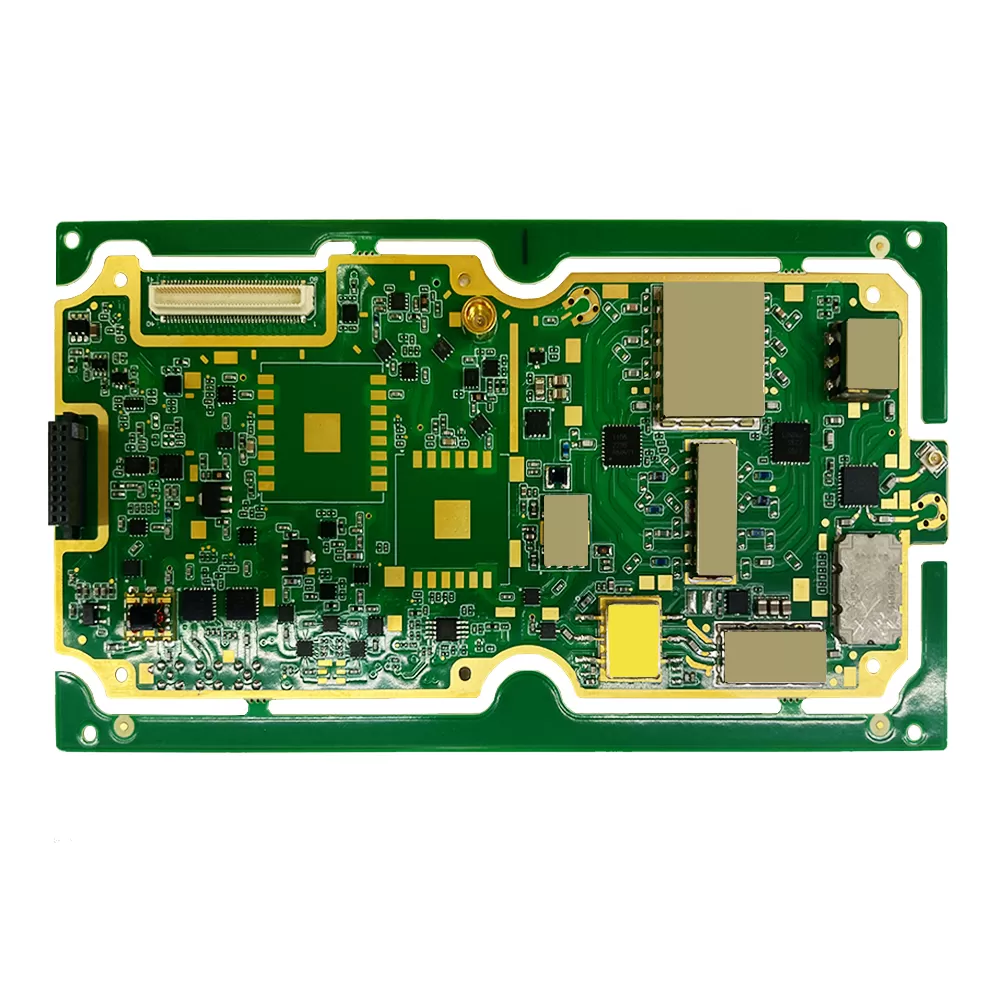

TMS320C6746EZCED4
Brand: Texas Instruments
Texas Instruments TMS320C6746EZCED4 is a power management component designed for AI Servers & Low-Altitude Economy (Drone and UAV) and related applications. In stock at Superb Automation — request a quote for competitive pricing and fast delivery.
Product Specifications
TMS320C6746EZCED4
Texas Instruments — Power Management & Signal Chain
Product Overview
The TMS320C6746EZCED4 from Texas Instruments is a power management / signal chain IC delivering high efficiency, precision regulation, and robust protection. Texas Instruments (TI) is a global leader in analog ICs, power management solutions, and embedded processors.
Superb Automation partners with leading brands including Qorvo, TI, ADI, XILINX, NVIDIA, Intel, ST, MACOM, Renesas, and Coilcraft to provide complete BOM and supply-chain solutions.
Key Features
- High-efficiency power conversion with low quiescent current
- Wide input voltage range with precision output regulation
- Integrated over-current, over-temperature, and short-circuit protection
- Small footprint packaging for space-constrained designs
- AEC-Q100 qualified options available for automotive applications
- Flexible sequencing and soft-start control
Key Specifications
| Input Voltage | V |
| Output Voltage | V |
| Output Current | A |
| Switching Frequency | kHz |
| Efficiency | % |
| Quiescent Current | µA |
| Topology | — |
| Package | — |
| Operating Temp | °C |
| Protection | — |
Applications
Industrial Automation
Automotive Electronics
Telecom Infrastructure
Server & Data Center Power
Medical Devices
Consumer Electronics
Request Quote — In Stock, 100% New & Original, Full Warranty
TMS320C6746EZCED4: a floating point DSP in a 361 ball package
The TMS320C6746EZCED4 is a fixed and floating point DSP from the C674x family, ordered in the ZCE ball grid package at the 456 MHz speed grade and rated from minus 40 to 90 C. It carries 32 kilobytes of level 1 program cache, 32 kilobytes of level 1 data cache and 256 kilobytes of level 2 memory that can be split between cache and directly addressed RAM.
Floating point changes what a filter chain costs. A 32 bit float multiply and accumulate takes one cycle per lane, and the instruction set includes single precision and double precision operations, so an algorithm written in C with floats runs without the scaling work that a fixed point device needs. For audio, sonar, radar and motor control, that is the difference between a port and a rewrite.
The peripheral set is wide: two external memory interfaces, one for DDR2 or mobile DDR and one for slower memories and peripherals, a universal parallel port, a multichannel audio serial port with sixteen serializers, USB 2.0 high speed, Ethernet MAC, three enhanced capture modules and a programmable real time unit subsystem.
Key data for the TMS320C6746EZCED4
| Core | C674x fixed and floating point, VLIW with eight functional units |
| Clock | 456 MHz on this grade at a 1.3 V core, 375 MHz at 1.2 V |
| Level 1 memory | 32 kilobytes program cache and 32 kilobytes data cache |
| Level 2 memory | 256 kilobytes, configurable as cache or mapped RAM |
| External memory | DDR2 and mobile DDR interface, plus a separate interface for NOR, NAND and SRAM |
| Audio | One multichannel audio serial port with sixteen serializers |
| Video and data | Universal parallel port, video port interface |
| Networking | Ethernet MAC compliant with IEEE 802.3 |
| USB | USB 2.0 high speed with integrated PHY |
| Control | Three enhanced capture modules, enhanced PWM, eQEP |
| Package | 361 ball NFBGA, ZCE, 16.00 mm by 16.00 mm |
| Temperature | Minus 40 to 90 C on the ZCE order code |
| Ordering | TMS320C6746EZCED4, 160 pieces per tray, nickel palladium gold finish |
Why the cache and RAM split is a software decision with a hardware cost
The level 2 block can be cache, or it can be memory that the program addresses directly, or a mixture. A signal chain that runs the same filter over a buffer wants cache, because the data is reused. A chain that streams samples once and never looks at them again wants mapped RAM, because cache filled with data that is never read again is wasted silicon.
Getting this wrong shows up as a processor that runs at half the expected speed with no obvious cause, and the fix is usually a linker change rather than a code change. It is worth measuring both arrangements on the bench before the product specification is fixed, because the result often decides whether the 375 MHz grade is enough.
The external memory interfaces add a second version of the same decision. DDR2 gives bandwidth for frame sized buffers; the slower interface is where the boot image and the configuration live. Both share pins with other peripherals, so the pin plan has to be made early, before the board is closed.
Floating point and the algorithms it makes practical
On a fixed point device, a filter with a wide dynamic range needs scaling, saturation handling and a coefficient format that is chosen for the worst case signal. On this part the same filter can be written in float, and the effort moves from numerical analysis to algorithm work.
Double precision is available but slower: two double precision multiplies every four cycles, compared with two single precision multiplies every cycle. That ratio matters for anything doing matrix work or long integration, and it usually pushes the implementation toward single precision with a correction step.
What the part does not do is remove the need to understand the signal chain. A float multiply is still one instruction, and a sample rate that is too high for the cache behaviour will still cost more than the arithmetic.
Where it fits in a build
Professional audio, sonar and acoustic processing, radar front end control, machine vision pre processing and industrial drives. The 361 ball package with a 0.8 mm pitch needs a board with enough layers to fan out, so it belongs in products where the board area is already committed.
The ZCE order code is rated from minus 40 to 90 C, which is narrower than the industrial parts around it. For a product that has to run inside a sealed enclosure in summer, the thermal calculation has to be done on the case temperature and not on the ambient of the room. The component obsolescence management page is where we track the life of a processor like this across a long programme, since the package and the speed grade both move over time.
The sourcing side of this part is covered on the component lead time solutions. For a DSP that a programme may have to hold for years, that page covers how buffer is sized and what is confirmed before a date is promised.
Questions we get on this code
What is the difference between the ZCE and ZWT packages? Both are 361 ball NFBGA and both are 16 mm square. The pinout and the thermal performance differ, and the temperature rating differs with the order code rather than with the package.
Can the part boot from SPI flash? Yes, through the boot loader in ROM, with the source selected by pins. A production board normally boots from SPI or NAND and leaves the host interface free.
How much DDR2 can it address? The interface is 16 bits wide and runs up to 156 MHz, which is enough for a frame buffer or an audio delay line, not for a general purpose operating system with a large heap.
Is the 375 MHz grade a different silicon? No, it is the same device at a lower core voltage, so the board has to supply 1.2 V instead of 1.3 V. The two grades are not interchangeable on the same board without a supply change.


