


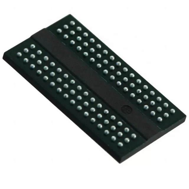
MT40A512M16TB-062E:R
The MT40A512M16TB-062E:R is an 8 Gb (1 GB) DDR4 SDRAM component from Micron Technology, organized as 512M × 16-bit and rated for DDR4-3200 (3200 MT/s, PC4-25600). Packaged in a compact 96-ball TFBGA, it delivers 12.8 GB/s of peak bandwidth in a dual-chip 32-bit embedded configuration — making it the go-to DRAM choice for ARM-based embedded SoCs (NXP i.MX8, Rockchip RK3568, Xilinx Zynq), networking equipment, and industrial computing platforms. The :R suffix designates tape-and-reel packaging for automated high-volume assembly.
Product Specifications
MT40A512M16TB-062E:R — 8Gb DDR4-3200 SDRAM by Micron Technology
The MT40A512M16TB-062E:R is an 8 Gb (1 GB) DDR4 SDRAM component from Micron Technology, organized as 512M × 16-bit and rated for DDR4-3200 (3200 MT/s, PC4-25600). Packaged in a compact 96-ball TFBGA, it delivers 12.8 GB/s of peak bandwidth in a dual-chip 32-bit embedded configuration — making it the go-to DRAM choice for ARM-based embedded SoCs (NXP i.MX8, Rockchip RK3568, Xilinx Zynq), networking equipment, and industrial computing platforms. The :R suffix designates tape-and-reel packaging for automated high-volume assembly.
Part Number Decoded — Field by Field
| Field | Value | Meaning |
|---|---|---|
| MT40A | Product Prefix | Micron Technology DDR4 SDRAM component |
| 512M | Row Address Space | 512 Mega-locations (NOT 512 MB). Each location = 16 bits (x16). Total = 512M × 16 = 8,192 Mb = 8 Gb = 1 GB per chip |
| 16 | Data Bus Width | x16 — 16 data lines (DQ0–DQ15), two data strobe pairs (UDQS, LDQS) |
| T | Die Technology | Specific manufacturing process node generation within Micron's DDR4 lineup |
| B | Die Version | B-die — second silicon generation within the T-process family |
| -062 | Speed Grade | tCK(min) = 0.625 ns. Clock = 1.6 GHz → Data Rate = 3200 MT/s (DDR4-3200). "062" encodes 0.625 ns |
| E | Die Revision | Fifth revision of the B-die silicon (A, B, C, D, E) |
| :R | Packaging Format | Tape-and-Reel (standard 3,000/4,000-unit reel). Colon is Micron's field delimiter. Without :R = Tray packaging |
| Temperature | No -IT suffix | Commercial: 0°C to +95°C TC (case temperature). Industrial variant = MT40A512M16TB-062E-IT:R (−40°C to +85°C) |
⚠️ Critical BOM Warning: "512M" in the part number does NOT mean 512 megabytes. It means 512 mega-addressable locations × 16 bits = 8 Gb = 1 GB per chip. Engineers who interpret "512M" as 512 MB will understate available memory by a factor of 2 — potentially specifying twice as many chips as needed.
Quick Specifications
| Parameter | Value |
|---|---|
| Manufacturer | Micron Technology |
| Part Number | MT40A512M16TB-062E:R |
| Mouser # | 340-471779-TRAY |
| Type | DDR4 SDRAM (Synchronous Dynamic Random-Access Memory) |
| JEDEC Standard | JESD79-4 Compliant |
| Density | 8 Gb = 1 GB per Chip |
| Organization | 512M × 16-bit |
| Speed Grade | DDR4-3200 (PC4-25600) |
| Data Rate | 3200 MT/s |
| Clock Frequency | 1,600 MHz |
| tCK (Minimum) | 0.625 ns |
| CAS Latency (CL) | 21 (at DDR4-3200) |
| tRCD / tRP | 21 cycles (13.125 ns) |
| tRAS (Minimum) | 47 cycles (29.375 ns) |
| Internal Banks | 8 Banks (2 Bank Groups × 4 Banks) — x16 Configuration |
| Row Addresses | A[0:14] = 15 bits = 32,768 Rows per Bank |
| Column Addresses | A[0:9] = 10 bits = 1,024 Columns per Row |
| Prefetch Architecture | 8n-Prefetch (128 Bits Internal Burst per Access) |
| Data Bus | 16-bit DQ (DQ0–DQ15) + 2 Differential DQS Pairs |
| VDD / VDDQ | 1.2 V (1.14 V – 1.26 V) |
| VPP (Wordline Boost) | 2.5 V (Required — Separate from VDD) |
| Active Read Current (IDD4R) | ~180–230 mA per Chip (at DDR4-3200) |
| Refresh | 8,192-Cycle Refresh at tREFI = 7.8 µs (TC ≤ 85°C) |
| ODT (On-Die Termination) | Programmable RTT_NOM, RTT_WR, RTT_PARK |
| ZQ Calibration | External 240 Ω (±1%) Reference Resistor Required |
| Package | 96-Ball TFBGA (Thin Fine-Pitch BGA) — 9 mm × 9 mm |
| Ball Pitch | 0.8 mm |
| MSL Rating | MSL-3 (Moisture Sensitivity Level 3) |
| Temperature Grade | Commercial: 0°C to +95°C TC (Case Temperature) |
| Industrial Variant | MT40A512M16TB-062E-IT:R (−40°C to +85°C) |
| Packaging Format | Tape-and-Reel (:R suffix, 3,000–4,000 units/reel) |
| Tray Variant | MT40A512M16TB-062E (without :R) |
| RoHS | Compliant |
Product Overview
The MT40A512M16TB-062E:R is one of Micron's highest-volume DDR4 SDRAM components for embedded applications. Built on Micron's B-die silicon, it represents the second-generation process node optimised for the DDR4-3200 speed bin — the sweet spot where bandwidth, power, and cost intersect for embedded system designers.
At DDR4-3200, a single chip delivers a theoretical peak bandwidth of 6.4 GB/s (3200 MT/s × 2 bytes). In the most common embedded configuration — two x16 chips on a 32-bit memory bus — the combined bandwidth reaches 12.8 GB/s, sufficient for 1080p video decode, multi-channel Gigabit Ethernet packet processing, and real-time DSP workloads on ARM Cortex-A and Xilinx Zynq platforms.
The DDR4 8n-prefetch architecture is the key enabler: while the external data bus runs at 1600 MHz (DDR), the internal DRAM array operates at just 200 MHz. Sense amplifiers and cell arrays cycle at 200 MHz; the external interface serializes 128-bit internal bursts into 16-bit external transfers over 4 clock cycles using double-data-rate signalling. This internal-to-external frequency ratio is the fundamental mechanism behind all modern DRAM speed scaling.
Key Features & Benefits
1 GB per Chip — High Density in Minimal Board Area
Each MT40A512M16TB-062E:R provides 1 GB of DDR4 memory in a single 9 mm × 9 mm FBGA-96 package. Two chips deliver 2 GB on a 32-bit bus — ideal for embedded SoCs that support 32-bit DDR4 interfaces but need sufficient memory for Linux-based applications:
NXP i.MX8M Plus / i.MX8M Nano — 32-bit DDR4, 2 GB with 2 chips
Rockchip RK3566 / RK3568 / RK3588 — 32-bit DDR4, 2–4 GB with 2–4 chips
Xilinx Zynq-7000 / Zynq UltraScale+ — 32-bit DDR4 PS DDR, 2 GB with 2 chips
Allwinner H6 / H616 — 32-bit DDR4, 2 GB with 2 chips
Intel Cyclone V SoC / Arria 10 SoC — 32-bit HMC DDR4, 2 GB with 2 chips
DDR4-3200: The Practical Performance Ceiling for Embedded DRAM
At tCK = 0.625 ns (1600 MHz clock), DDR4-3200 represents the highest JEDEC-standard speed grade commonly deployed in embedded systems. Performance characteristics at this speed bin:
CAS Latency: CL21 (13.125 ns absolute) — actually lower absolute latency than DDR4-2133 CL15 (14.06 ns)
Row-to-Column Delay (tRCD): 21 cycles (13.125 ns)
Row Precharge (tRP): 21 cycles (13.125 ns)
32-bit Peak Bandwidth: 12.8 GB/s (dual-chip, single-rank)
64-bit Peak Bandwidth: 25.6 GB/s (quad-chip, single-rank)
For designs where DDR4-3200 timing margin is tight (long PCB traces, elevated temperature), the part can be operated at lower JEDEC speeds (DDR4-2666, DDR4-2400) by configuring the memory controller — often improving signal integrity without silicon changes.
x16 Organization: Fewer Chips, Simpler Layout
The x16 data bus width means each chip provides 16 DQ lines — exactly half of a typical 32-bit embedded SoC memory interface. Two chips complete the bus with no wasted data lanes. This is architecturally cleaner than using x8 chips (which would require 4 chips for a 32-bit bus) and reduces PCB routing complexity, BOM line items, and assembly cost.
The trade-off: x16 devices have 8 internal banks (2 bank groups × 4 banks) versus 16 banks for x4/x8 devices. For embedded workloads with predominantly sequential access patterns — video frame buffers, network packet buffers, filesystem caches — this bank count is fully adequate.
Essential VPP 2.5V Rail — Don't Overlook It
DDR4 introduced a dedicated VPP = 2.5V supply rail for the wordline boosting circuitry — a critical difference from DDR3 that traps designers migrating existing layouts. VPP must be present and stable before VDD/VDDQ power up. The power sequencing requirement is explicit: VPP ramps first, then VDD/VDDQ. A design that omits the VPP rail will show no memory response during initialization — a symptom easily confused with a controller configuration or signal integrity problem.
If your PCB has no existing 2.5V rail, add a small LDO or charge pump dedicated to VPP. The current requirement is modest (~10–50 mA per chip), but the sequencing order is mandatory.
Programmable On-Die Termination (ODT)
DDR4 ODT is independently programmable for three operating states: RTT_NOM (nominal termination during idle), RTT_WR (write termination), and RTT_PARK (park termination). Values are selected via Mode Register writes during controller initialization. Correct ODT settings are essential for signal integrity at DDR4-3200 — especially in multi-rank configurations where the terminating rank changes dynamically.
PCB Layout & Design Guidelines
Power Supply Sequencing
DDR4 power-up sequence (mandatory):
VPP (2.5V) — must reach operating range first
VDD / VDDQ (1.2V) — after VPP is stable
RESET# — hold low for ≥ 200 µs after VDD/VDDQ stable
Release RESET# → CKE high after tXPR
Decoupling Strategy
100 nF X5R/X7R ceramic capacitors within 2 mm of every VDD and VDDQ ball on each chip
4.7–10 µF bulk capacitance per chip per supply domain
100 nF per VPP ball (lower current, but high-frequency noise sensitive)
PCB Trace Routing (32-bit, 2-Chip Configuration)
| Signal Group | Impedance | Match Tolerance |
|---|---|---|
| CK_t / CK_c (Clock) | 85–100 Ω Differential | ±5 mil within pair |
| DQS_t / DQS_c (Data Strobe, per byte) | 85–100 Ω Differential | ±5 mil within pair |
| DQ[0:15] per Byte Lane | 40–50 Ω Single-Ended | ±15 ps within byte lane (~±3 mm on FR4) |
| Address / Command / Control | 40–50 Ω Single-Ended | ±50 ps |
ZQ Calibration Resistor
Connect a 240 Ω (±1%) resistor from the ZQ pin to ground on each chip. The resistor provides the reference impedance for on-die output driver calibration. Incorrect value or excessive trace length between the pin and the resistor degrades ODT accuracy, compromising signal integrity at DDR4-3200 speeds.
Controller Initialization Sequence
After RESET# deasserts, assert CKE high after tXPR
Write Mode Registers in order: MR2 → MR3 → MR1 → MR0
ZQ Calibration Long (ZQCL)
Write Leveling (compensates fly-by clock-to-strobe skew)
DQ-DQS Training — always enable controller training at DDR4-3200
Verify training pass before declaring the interface functional
⚠️ Common failure mode: Designs that pass at room temperature but show random bit errors at elevated temperature are almost always traced to insufficient DQ-DQS alignment margin. At tCK = 0.625 ns, the setup/hold window is tight — enable the controller's DQ-DQS training algorithm and verify training completion before shipping.
Target Applications
Embedded Linux Single-Board Computers
Two MT40A512M16TB-062E:R chips provide 2 GB DDR4 on a 32-bit bus — the standard memory configuration for NXP i.MX8M, Rockchip RK356x, and TI AM62x SBCs running Yocto, Buildroot, or Debian. The 12.8 GB/s bandwidth supports simultaneous HDMI display, Gigabit Ethernet, and NVMe SSD I/O.
Networking Equipment
Enterprise Wi-Fi 6 access points, 5G CPE routers, and SD-WAN appliances use DDR4-3200 for line-rate packet buffering and deep packet inspection (DPI) tables. Two to four MT40A chips on a 32-bit or 64-bit bus provide 2–4 GB with deterministic, low-latency access — critical for real-time forwarding.
FPGA-Based Systems (Xilinx / Altera)
The Xilinx Zynq-7000 Processing System DDR controller and Zynq UltraScale+ MPSoC DDR subsystem are designed for standard JEDEC DDR4 components. The MT40A512M16TB-062E:R is validated across the Zynq ecosystem and supported by Xilinx Vivado Memory Interface Generator (MIG) presets.
Industrial HMIs & Edge Gateways
Panel PCs, protocol converters, and edge AI gateways running Linux require reliable, long-lifecycle DRAM. Micron's embedded DRAM roadmap provides multi-year availability commitments that align with industrial product lifecycles. The commercial temperature range (0–95°C TC) covers most indoor industrial deployments; the -IT variant extends to outdoor/automotive-adjacent environments.
Digital Signage & Media Players
4K video decode framebuffers and GPU texture memory benefit from the 12.8 GB/s peak bandwidth of a dual-chip 32-bit DDR4-3200 configuration. Eight MT40A chips on a 64-bit bus provide 8 GB for multi-display digital signage controllers.
Automotive Infotainment & ADAS (Industrial Variant)
The industrial temperature variant (MT40A512M16TB-062E-IT:R, −40°C to +85°C) targets automotive-adjacent applications: IVI head units, telematics control units, and advanced driver-assistance ECU data buffers. For full AEC-Q100 qualification, consult Micron's automotive-grade DDR4 portfolio.
MT40A512M16 Variant Comparison
| Part Number | Data Rate | CAS Latency | Temperature | Package |
|---|---|---|---|---|
| MT40A512M16TB-062E:R | DDR4-3200 | CL21 | 0°C to +95°C | 96-FBGA, T&R |
| MT40A512M16TB-062E | DDR4-3200 | CL21 | 0°C to +95°C | 96-FBGA, Tray |
| MT40A512M16TB-062E-IT:R | DDR4-3200 | CL21 | −40°C to +85°C | 96-FBGA, T&R |
| MT40A512M16TB-083E:R | DDR4-2400 | CL17 | 0°C to +95°C | 96-FBGA, T&R |
| MT40A512M16TD-062E:R | DDR4-3200 | CL21 | 0°C to +95°C | 96-FBGA, T&R (T-die) |
| MT40A512M16LY-062E:R | DDR4-3200 | CL21 | 0°C to +95°C | 78-FBGA, T&R (LP variant) |
Frequently Asked Questions
Why does the part number say "512M" if the chip is 1 GB?
"512M" in Micron's DDR4 naming convention refers to the row address space — 512 mega-locations, each 16 bits wide (the x16 part of the number). Total capacity = 512M × 16 bits = 8,192 megabits = 8 Gb = 1 GB per chip. This is the single most common misunderstanding that leads to BOM errors. Always convert: density in Gb = row-address-M × data-width / 1024.
What is the difference between MT40A512M16TB-062E and MT40A512M16TB-062E:R?
Identical silicon. The colon and "R" suffix designate packaging format only: MT40A512M16TB-062E ships in trays; MT40A512M16TB-062E:R ships in tape-and-reel. For prototype and engineering builds, order Tray. For any production run using automated pick-and-place, specify :R (tape-and-reel). Ordering the wrong packaging format for a production run causes avoidable procurement delays.
Is the MT40A512M16TB-062E:R obsolete?
Micron's website shows the -J suffix variant (MT40A512M16TB-062E-J) as obsolete. The :R variant is a different SKU. As of mid-2026, the :R variant is available through trusted distribution including RS Components and Mouser. As with all DRAM components, verify current lifecycle status with Micron or your trusted supplier before locking in a new design.
Can the MT40A512M16TB-062E:R operate below DDR4-3200?
Yes. Although rated for DDR4-3200, the chip can operate at any lower JEDEC speed (DDR4-2666 CL19, DDR4-2400 CL17, DDR4-2133 CL15) by configuring the memory controller accordingly. Running below the rated speed often improves timing margin and signal integrity — useful for designs with longer PCB traces, elevated operating temperature, or multi-rank configurations where loading is higher.
What is the difference between the TB (B-die) and TD (T-die) variants?
Both are Micron x16 DDR4-3200 parts at 8 Gb density with the same 96-ball FBGA package. The TB variant uses Micron's B-die (second-generation T-process silicon); the TD variant uses Micron's T-die (a different process generation). In practice, the two are functionally interchangeable — both meet the same JEDEC DDR4-3200 timing specifications. Designers may encounter one or the other in the supply chain; treat them as drop-in equivalents.
What is the minimum order quantity (MOQ)?
Contact SUPERB Automation for a tailored quote. We support prototype quantities (single chips on tray) through full production volumes (tape-and-reel). Send your BOM to pcba@superb-tech.com — we quote within hours.
Does the x16 MT40A part work with x8-only DRAM controllers?
No. The memory controller must be configured for the connected DRAM's data bus width. An x16 chip uses 16 DQ lines per chip — most embedded SoCs support configurable DRAM data widths (x8, x16, x32) via register settings. Verify your SoC's DDR subsystem supports x16 organization before finalising the BOM. For controllers that only support x8 DRAM, use Micron's MT40A1G8 (x8, 8 Gb) or equivalent x8-organized parts.
Ordering Information
| Orderable Part Number | Package | Packaging | Temperature |
|---|---|---|---|
| MT40A512M16TB-062E:R | 96-FBGA (9×9 mm) | Tape & Reel | 0°C to +95°C |
| MT40A512M16TB-062E | 96-FBGA (9×9 mm) | Tray | 0°C to +95°C |
| MT40A512M16TB-062E-IT:R | 96-FBGA (9×9 mm) | Tape & Reel | −40°C to +85°C |
Design Resources
Datasheet: Micron MT40A512M16TB — TN-46-16 (DDR4 SDRAM Component Data Sheet)
JEDEC Standard: JESD79-4 — DDR4 SDRAM Standard (timing, electrical, and mechanical specifications)
Application Note: Micron TN-40-07 — "DDR4 Point-to-Point Design Guide" (PCB layout, SI, power delivery)
IBIS Model: Available from Micron for signal integrity simulation at DDR4-3200 speeds
Footprint / Symbol: Available from SnapEDA, Ultra Librarian, EasyEDA — 96-ball FBGA, 0.8mm pitch
Controller Reference: Vendor-specific DDR4 initialization and training sequences (Xilinx MIG, NXP DDR Tool, Rockchip DDR bin)
Request a Quote
SUPERB Automation supplies genuine Micron MT40A512M16TB-062E:R DDR4 SDRAM with full traceability and competitive lead times. From prototype tray quantities for new board bring-up to production tape-and-reel volumes, we deliver.
Send your BOM or inquiry to pcba@superb-tech.com — we quote within hours. For full PCBA projects including DDR4 memory sub-system assembly, include your Gerber files for a complete turnkey quote.
SUPERB Automation — We Make It Real. Since 2000.
