


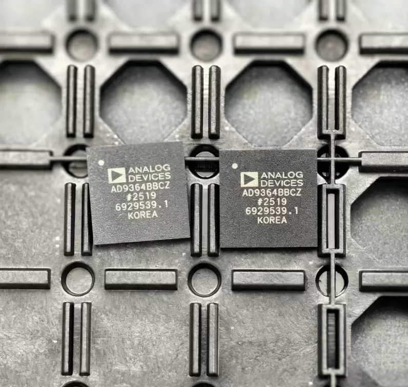

AD8622ARZ
Brand: Analog Devices
Analog Devices AD8622ARZ is a analog & mixed-signal component designed for Instrumentation and related applications. In stock at Superb Automation — request a quote for competitive pricing and fast delivery.
Product Specifications
AD8622ARZ
Analog Devices — Analog & Mixed-Signal ICs
Product Overview
The AD8622ARZ from Analog Devices is a high-performance analog / mixed-signal IC providing precision signal acquisition, conversion, and conditioning. Analog Devices (ADI) is a world leader in high-performance analog, mixed-signal, and DSP ICs for instrumentation, healthcare, automotive, and communications.
Superb Automation partners with leading brands including Qorvo, TI, ADI, XILINX, NVIDIA, Intel, ST, MACOM, Renesas, and Coilcraft to provide complete BOM and supply-chain solutions.
Key Features
- High-resolution data conversion with excellent SNR and THD
- Wide dynamic range and high linearity across operating conditions
- Integrated voltage reference with low temperature drift
- Flexible digital interface — SPI, I2C, or parallel options
- Industrial/automotive temperature range with guaranteed specs
- Low power consumption with power-down modes
Key Specifications
| Resolution | bits |
| Channels | — |
| Sample Rate | kSPS |
| Interface | — |
| Supply Voltage | V |
| Operating Temp | °C |
| Package | — |
| INL | LSB |
| SNR | dB |
| THD | dB |
Applications
Precision Instrumentation
Industrial Process Control
Medical Imaging & Diagnostics
Automotive Sensor Interfaces
Communications Infrastructure
Test & Measurement
Request Quote — In Stock, 100% New & Original, Full Warranty
AD8622ARZ: dual 125 microvolt precision amplifier at 215 microamps per channel
The AD8622ARZ is the two channel member of the AD8622/AD8624 low power precision family in an 8-lead SOIC_N body. Each amplifier holds a 125 uV maximum offset and 1.2 uV/C maximum drift while drawing 175 uA typical at a plus or minus 2.5 V supply, which is the combination that decides a battery instrument: the offset is small enough for a 16-bit converter and the current is small enough for a 4 mA loop.
Published values
| Parameter | Value |
|---|---|
| Offset voltage, 25 C | 10 uV typical, 125 uV maximum |
| Offset voltage drift | 0.5 uV/C typical, 1.2 uV/C maximum, -40 to +125 C |
| Input bias current | 30 pA typical, 200 pA maximum |
| Input offset current | 25 pA typical, 200 pA maximum |
| Supply current per amplifier | 175 uA typical, 225 uA maximum at +-2.5 V; 215 uA typical at +-15 V |
| Gain bandwidth | 540 kHz at +-2.5 V, 560 kHz at +-15 V |
| Slew rate | 0.28 V/us at +-2.5 V, 0.48 V/us at +-15 V |
| Voltage noise density | 12 nV/root Hz at 1 kHz, 0.2 uV p-p over 0.1 to 10 Hz |
| CMRR | 110 dB minimum at +-2.5 V, 125 dB minimum at +-15 V |
| Input voltage range | -1.3 V to +1.3 V on a +-2.5 V supply |
| Output swing | 2.45 V minimum high and -2.45 V maximum low into 100 k to ground |
| Short circuit current | 30 mA |
| Supply range | +-2.0 V to +-18 V |
| Package | 8-lead narrow body SOIC_N |
What 125 uV costs in converter codes
On a 5 V span one 16-bit code is 76.3 uV, so the 125 uV maximum offset is 1.6 codes before anything else is counted. Drift adds 1.2 uV/C times 165 C, which is 198 uV or 2.6 codes, so a channel that is trimmed at 25 C and then runs hot carries about four codes of offset error. That is a real number for a 16-bit measurement and it is the reason the part is described as precision rather than as an instrumentation amplifier substitute.
For a 12-bit converter on the same span one code is 1.22 mV, so the same offset is a tenth of a code and the AD8622 disappears from the error budget. The part earns its price in a 16-bit or 18-bit channel, and in a 12-bit channel a 1 mV class part does the same job for less.
Where 540 kHz stops
At a closed loop gain of 100 the usable bandwidth is 5.4 kHz, and a 2 V step slews at 0.28 V/us, which is 7.1 us before the loop begins to settle. A scanner that gives each channel 1 ms is comfortable with that; a channel that has to settle in 50 us is not. The two numbers, bandwidth and slew, have to be checked together because a small signal and a full scale step behave differently.
Output swing is 2.45 V minimum into 100 k, which is 50 mV below the positive rail. Into a 10 k load the swing is smaller, and a 16-bit converter driven directly by this amplifier loses the top and bottom few hundred codes. Where the full span matters, the output goes through a buffer or the converter is driven differentially with two of these amplifiers.
The input window is not rail to rail
The input common mode range is -1.3 V to +1.3 V on a plus or minus 2.5 V supply, which is a 2.6 V window centred on ground. A single supply 5 V board that swings its signal from 0 V to 5 V is outside that window at both ends, so the part belongs on a split supply or on a signal that is biased at mid rail with a gain that keeps it inside the window. The 200 pA bias current into a 1 MOhm source is 0.2 mV, which is larger than the offset the part was bought for, so a high impedance sensor needs a guard or a buffer in front of it.
Sourcing notes for this family: the amplifier cross reference holds the cross references, how to verify a drop in replacement is the pre substitution check, and component lead time solutions is what we use when the part on the drawing is not on the shelf.
Two questions buyers ask
Can the AD8622ARZ replace an AD8628ARZ in a thermocouple channel? The pinout of an 8-lead SOIC dual and an 8-lead SOIC single are not the same circuit, so it is not a socket swap: the AD8622 draws 175 uA per channel with a 125 uV offset, the AD8628 draws 1 mA with a 1 uV offset. If the channel needs a microvolt offset, the AD8622 is the wrong part; if the budget is microamps, the AD8628 is.
What supply does this part need for a 0 V to 5 V signal? A plus or minus 2.5 V split supply with the signal biased at 0 V, or a plus or minus 5 V supply with the signal biased at mid rail. A 5 V single supply does not give the input window room at 0 V and 5 V.