

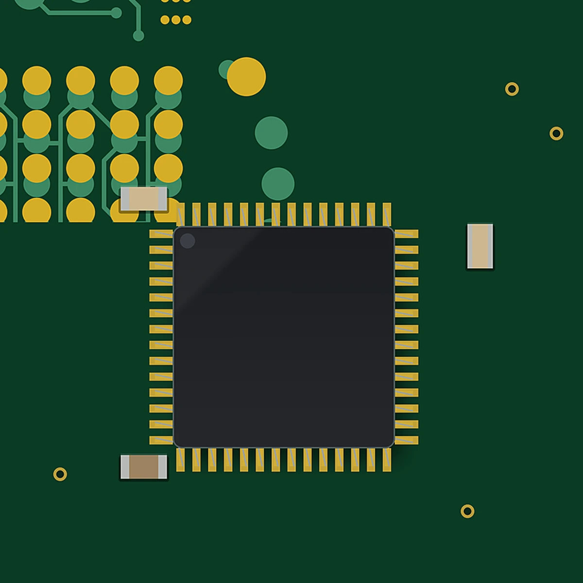
Medical Aesthetic RF Device PCBA


Product Specifications
What is actually inside an aesthetic RF device
Skin tightening, body contouring and RF microneedling machines are not one board. They are usually three to four boards working as one system, and each has a different manufacturing risk.
- RF power board. DC bus, half or full bridge, resonant network and transformer. Typical operating frequencies are 1 MHz to 6.78 MHz, with 40.68 MHz used in some handpieces and 2.45 GHz in fractional RF tips. Output is commonly 30 W to 200 W into a handpiece load that changes with contact area and gel.
- Control board. MCU or DSP, impedance sensing, temperature loop, user interface and treatment logging.
- Handpiece board. The matching network, temperature sensor and electrode contact, sitting at the end of a cable that adds capacitance and inductance the board never sees on the bench.
- Patient safety board. Return electrode contact monitoring and the isolation barrier between the applied part and the mains side.
Most of the cost of getting these boards wrong is not in the components. It is in the field: a unit that trips a leakage test, drifts in output power, or fails after the coating is applied.
Five failure modes we build the process around
1. Flux residue raising leakage current. Cosmetic RF units are tested for patient leakage at 100 µA or lower on the applied part. No-clean flux left on a high-impedance sense node can pull that number up after a few weeks of humidity. We either run an aqueous wash with ionic contamination checking, or specify a coating over the sense network, and we tell you which route the design allows before we build.
2. Matching network tolerance moving the output power. A resonant network built with 5% capacitors drifts. We place 1% parts where the BOM calls for them, keep the network away from the reflow shadow of tall parts, and measure output into a dummy load at final test, not just continuity.
3. Voids under the RF power device. A MOSFET or LDMOS with 30% voiding under the thermal pad runs hot and dies early. We X-ray the thermal pad, hold voiding to the limit agreed in the DFM report, and adjust the reflow profile per board thickness rather than running one profile for everything.
4. The handpiece cable changes the load. A board tuned on the bench into 50 Ω can show high VSWR with the real cable and handpiece attached. Final test runs with the production cable and a load that represents the electrode, using the limits you give us.
5. Coating on a contact that must stay clean. Selective coating protects the high-voltage and high-impedance areas, but it also creeps into connector cavities and pressure contacts. Every programme gets a keep-out drawing, and the coating operator works from that drawing, not from memory.
Process data: what we actually run
| Item | Capability |
|---|---|
| Placement | 0201 passives and 0.35 mm pitch QFP / QFN |
| Minimum trace and space | 5 mil (0.127 mm) in routine production |
| Inspection | AOI on 100% of boards, X-ray on QFN, BGA and thermal pads |
| Coating | Selective conformal coating, potting and full dip, with masking per drawing |
| Assembly scope | SMT, through-hole, cable harness and box build |
| Electrical test | DC, functional, hipot and leakage current with a fixture built for the programme |
| RF verification | Output power and return loss into a dummy load to your limits; full RF characterisation through our RF lab partner when the spec needs it |
| Quality system | ISO 9001 |
| Burn-in | Not offered in house. If the protocol requires it, we say so before quoting and it is arranged separately. |
The build and test sequence
- DFM review before tooling. Pad geometry, creepage and clearance against the isolation class, coating keep-outs, panel design for a small board. You get the report in writing, with the items we will not sign off.
- First article. One panel built, photographed and measured, then held until you approve it.
- Production. Solder paste, placement, reflow, AOI, through-hole and selective solder where the design needs it.
- X-ray. Thermal pads, QFN and any BGA, with void percentage recorded.
- Coating and cure. Masking verified against the keep-out drawing, UV inspection after cure.
- Electrical and safety test. Functional into a dummy load, hipot, leakage current. Fixture and limits agreed at quote stage.
- Final QA and traceability. Panel and date code recorded, test data stored against the lot.
Compliance: what we do and what stays with you
Designs in this category are usually assessed against IEC 60601-1 for general safety, IEC 60601-1-2 for EMC and, where the function is RF cutting or coagulation, IEC 60601-2-2. Those are design and certification responsibilities of the legal manufacturer. What we control is what can be controlled in manufacturing: creepage and clearance as drawn, isolation barrier integrity through assembly, coating coverage, voiding, and documented test results.
We hold ISO 9001. If your device needs an ISO 13485 supplier, tell us at the enquiry stage so the quality agreement and the documentation set are agreed before the first panel, not after.
What to send us
- Gerber and drill files, plus the fabrication drawing or stack-up with copper weight, board thickness, surface finish and TG.
- BOM with manufacturer part numbers and any approved alternates. Do Not Substitute items are flagged and respected.
- Isolation class and the creepage and clearance you need on the applied part.
- Test limits: leakage current, hipot voltage, output power window, return loss.
- Handpiece and cable specification, if final test has to run with them connected.
- Coating keep-out drawing, if the assembly is coated.
Send the Gerber and the BOM first. You will get a DFM report and a price with the process route written out, and the list of what we test and what we do not.
Questions we get asked
Can you build very small boards? Yes. Two-layer boards around 15 × 17 mm with 3.0 mm mounting holes, 0.43 mm plated holes and 5 mil traces are normal work for us. Small boards are panelised, and the panel is quoted with the board.
Do you tune the matching network? No. Matching values come from your design and your handpiece. We build them to tolerance and verify output power and return loss against the limits you set.
Can you do the handpiece and cable as well? Yes, as box build, if the harness drawing and connector specification are supplied.
What quantity do you start from? We quote the quantity you actually need, from prototype panels upward. Tell us the annual volume as well, because it changes the fixture and panel decisions.