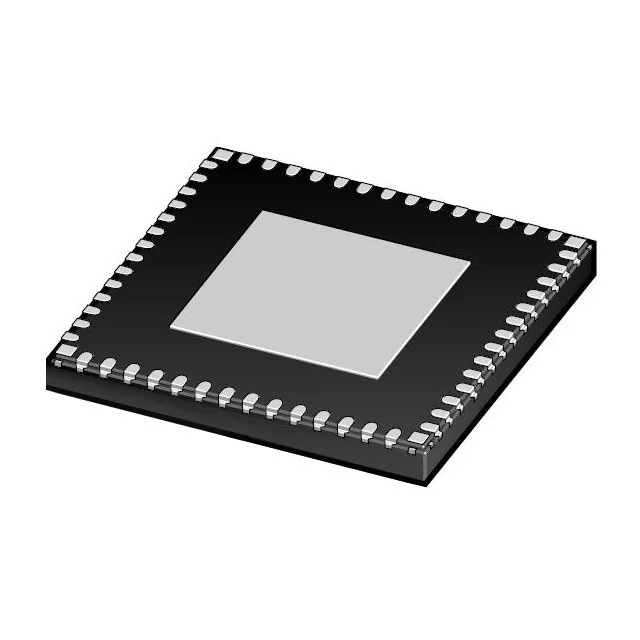

An RF power transistor is usually the last part anyone wants to replace, and the first one the buying team asks about. A line card goes end of life and the search for an RF power transistor cross reference starts from a part number that has been in the same amplifier for a decade.
The list that comes back looks reasonable: same flange, similar output power, similar frequency range. Then the amplifier is built and the gain is 1.5 dB low at the top of the band, or the drain current runs away as the case warms up.
Why a package match is not a cross reference
RF power transistors are matched to their circuit in a way that low frequency parts are not. Many carry internal matching networks, so the impedance presented to the board is set inside the package. Two devices with the same flange and the same headline output power can have a different input impedance, a different gain slope across the band, and a different bias point for the same quiescent current.
The bias network is the second trap. A replacement with a lower gate threshold or a different gate capacitance can turn a stable bias loop into a slow one, so the amplifier passes on the bench and drifts as it heats. The third trap is thermal. The same outline does not mean the same junction to case resistance, and a smaller die in an identical flange runs hotter at the same dissipated power.
None of this appears in a title specification. It appears at the band edges, at temperature, and after a few hundred hours in the field.
The parameters that decide an RF power transistor cross reference
| Parameter | Why it decides the outcome | What a weak comparison looks like |
|---|---|---|
| Frequency range and gain flatness | The replacement has to hold gain across the whole band, not only at the centre | Gain matched at one test frequency, then a roll off at the band edge that eats the link margin |
| Output power at compression | P1dB and saturation set the headroom available for the modulation in use | Same saturated power quoted, less back off before distortion rises |
| Input and output impedance | Internal matching decides what the board has to present to the device | Same package, different matching, so the existing network no longer tunes the band |
| Drain efficiency | Efficiency sets the heat that the flange and the heatsink have to move | Comparable output power at several points more dissipation and a hotter case |
| Bias point and threshold | The gate or base network has to reach the same quiescent current with the same control loop | Bias that holds on the bench, then drifts at temperature or after a supply transient |
| Thermal resistance | Junction to case decides the die temperature at a given dissipation | Same outline, higher thermal resistance, shorter life at the same operating point |
| Package, flange and lead form | Mechanical fit: screw pattern, lead position, clamp or solder mounting | Fits the heatsink but needs a different lead form or a new clamp |
| Robustness and grade | VSWR tolerance, ESD class and the temperature grade the programme requires | Commercial grade where the build needs industrial or military screening |
How SUPERB PCBA builds the comparison
Send the original part number, the amplifier it sits in, and the quantity per year. The reply is a line by line comparison against the parameters above, with the differences that matter to your circuit marked, and with any point the datasheet does not settle written back as a question plus the condition needed to close it. A part that has gone end of life is handled through the routes collected in the obsolete part cross reference hub.
Where the comparison points to a device that fits the outline but needs a small change to the matching network or the bias loop, that change is checked with the board in hand. SUPERB Assembly runs first article inspection against the released data, with 3D SPI before reflow and 3D AOI after it, X-ray inspection in 2D and CT mode with voiding below 5 percent, and in circuit and functional test on fixtures approved by your team, under IPC-A-610 Class 2 and Class 3 and IPC-7095 for area array work.
The board side of the same build is supported from 500 MHz to 77 GHz, with lines down to 0.05/0.05 mm, impedance held to plus or minus 5 percent and to plus or minus 2 percent where the circuit needs it, Rogers RO4003C, RO4350B and RO4835, Taconic RF-35, TLY-5 and CER-10, mixed RF and FR-4 stack ups, and up to 68 layers. This matters for a power transistor change, because a different matching usually means a different board, and the device and the board should not sit in two separate orders.
Provenance is checked before any replacement enters a build: reel counting by X-ray, package and marking inspection, and decapsulation where the risk justifies it. Verified lots carry a 730 day warranty, and a substitution only enters the BOM after written approval from your side. Background reading: pin to pin cross reference, a worked GaAs RF power transistor replacement, and the families listed under RF and microwave devices.
When the replacement needs a board change
Some candidates are electrically suitable and mechanically impossible: a different lead form, a flange that does not reach the heatsink pattern, a device that needs a clamp where the old one was soldered. Others fit but move the bias network outside its stable range. Both cases are cheaper to resolve inside one build than across two suppliers and a re-qualification cycle.
A practical rule is to fix the acceptance criteria while the shortage is still being discussed, before the line is waiting.
RF power transistor cross reference questions
Can a device marked not recommended for new designs still be bought?
Usually yes, while it remains in the production plan and in the channel. The useful step is to secure the quantity the programme needs and to qualify a second option while the part is still easy to find.
Is a part with the same flange and power rating a drop in replacement?
No. Flange and output power are the entry conditions. Input impedance, gain slope, bias point and thermal resistance decide whether the amplifier still meets its specification.
How is a candidate proved before it goes into a build?
On hardware: a comparison table first, then first article inspection and functional test on the assembly, with the test data kept against the lot. Where the circuit allows, the candidate is run at the temperature corners as well.
What happens if no cross reference can be proved?
Then the options are covered stock from the final order window, verified lots with documented examination, or a change to the matching network around a device that is still in production. All three are quoted with their test impact.
Next step
Send the original part number, the amplifier or assembly it belongs to, and the quantity per year. You get the comparison table with the differences marked, the candidate list with availability, and the test plan needed to release the change.