



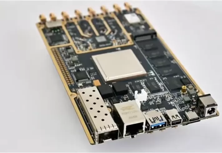
RF Transceiver Board PCBA - ADRV9009 assembly
RF Transceiver Board PCBA. RF PCBA, Power Amplifier, LNA, RF Front-End, Phased Array, Beamforming, Antenna Array, Frequency Synthesizer, Rogers PCB
Product Specifications
SDR Zynq + ADRV9009 PCBA Assembly — RF Transceiver Board Manufacturing
Full-turnkey PCBA for software-defined radio and RF transceiver boards. XCZU15EG FPGA with ADRV9009 wideband transceiver on Rogers/Megtron hybrid stack-up. 16-bit ADC, JESD204B, EVM-tested.
Featured Build: Zynq UltraScale+ + ADRV9009 SDR Platform
This software-defined radio board integrates a Xilinx Zynq UltraScale+ XCZU15EG FPGA (1156-ball BGA, 35 x 35 mm) with an Analog Devices ADRV9009BBCZ wideband RF transceiver (75 MHz to 6 GHz, 196-ball CSP BGA) on a single compact PCB. It represents the highest class of mixed-technology PCBA — combining large-format BGAs, fine-pitch RF packages, multi-voltage power management, DDR4 memory, and precision analog front-end traces on a board measuring 160 x 100 mm.
SDR Platform Specifications
| Parameter | Specification |
|---|---|
| FPGA | Xilinx Zynq UltraScale+ XCZU15EG-2FFVB1156I |
| CPU Cores | Quad ARM Cortex-A53 @ 1.33 GHz + Dual ARM Cortex-R5F @ 533 MHz |
| RF Transceiver | ADRV9009BBCZ, 75 MHz – 6 GHz, 2T2R |
| ADC / DAC Resolution | 16-bit ADC, 14-bit DAC |
| Signal Bandwidth | TX 450 MHz, RX 200 MHz per channel |
| TX Output Power | 22 dBm linear (25 dBm max) |
| Memory | PS DDR4 4 GB + PL DDR4 4 GB (eight 96-ball BGA devices) |
| Storage | 32 GB eMMC + 512 Mb QSPI Flash |
| Interfaces | USB 3.0, GbE, Mini DP, SSD NVMe, SD Card, GPS, JTAG, UART |
| Expansion I/O | 32 GPIO |
| Power Input | 12 V / 3 A DC |
| Operating Temperature | -40C to +85C (industrial range) |
| Board Dimensions | 160 x 100 mm |
SUPERB Capability: We have assembled multiple Zynq + ADRV9009 SDR platforms. Our PCBA workshop handles 1156-ball large-format BGAs, 0.8 mm pitch CSP RF packages, dual-side SMT with mixed through-hole connectors, and full functional test including RF loopback and DDR memory verification — all under one roof.
RF Transceiver Board Architecture
The RF transceiver board PCBA provides a complete frequency conversion engine that translates between baseband IQ signals and RF carriers from 700 MHz to 3.8 GHz — or up to 6 GHz for wideband SDR platforms. Designed for 5G NR remote radio heads, software-defined radios (SDR), and tactical communication terminals, this assembly integrates quadrature modulators and demodulators, programmable-gain amplifiers, and frequency synthesizers on a single precision PCB.
The differential IQ interfaces achieve carrier suppression exceeding 45 dBc and sideband suppression better than 40 dBc across the full operating band. Programmable conversion gain from 25 to 35 dB enables dynamic range optimization under varying channel conditions. For SDR applications using the ADRV9009, the JESD204B serial interface provides deterministic latency and multi-chip synchronization across all transceiver lanes.
General Specifications
| Parameter | Specification |
|---|---|
| Layer Count | 8–10 layers (digital + RF hybrid) |
| Material | Rogers 4003C / Megtron 6 hybrid |
| Surface Finish | ENIG / Immersion Silver |
| Min. Trace/Space | 4/4 mil (digital), 8/8 mil (RF) |
| Impedance Control | 50 Ohm single-ended, 100 Ohm differential, +/-10% |
| Frequency Range | 700 MHz – 6 GHz (application-dependent) |
| Conversion Gain | 25–35 dB (programmable in 1 dB steps) |
| Input IP3 | +28 dBm (high-linearity mode) |
PCBA Assembly Challenges
BGA Placement and Reflow for FPGA + RF Packages
The 1156-ball ZU15EG BGA (35 mm x 35 mm) and 196-ball ADRV9009 CSP BGA (12 mm x 12 mm) present very different thermal masses on the same board. The reflow profile must bring the FPGA balls to full liquidus without overheating the smaller RF package. A 12-zone nitrogen-purge oven with a ramp-soak-spike profile optimized for the largest thermal mass ensures uniform soldering across all BGA devices.
RF Signal Path Integrity
Assembling an integrated transceiver board demands meticulous isolation between the high-power LO path and the sensitive IQ baseband inputs. The quadrature modulator and demodulator ICs typically arrive in 6 mm x 6 mm or larger QFN packages with exposed thermal pads; these require Type 4 solder paste (20-38 um particle size) applied through a 4 mil laser-cut stencil with rounded aperture corners to ensure consistent paste release.
The LO distribution network uses Wilkinson dividers implemented as surface-mount discrete components or embedded stripline structures. Symmetric placement and matched trace lengths to within +/-5 mil are essential to maintain quadrature phase accuracy. Digital spur coupling from the SPI control bus and JESD204B SerDes lanes into the RF chain is suppressed through guard rings, grounded via fences, and buried stripline routing of the LO signals on inner layers.
Post-Reflow Inspection
Post-reflow, 3D X-ray inspection verifies the thermal pad solder joint integrity under all QFN and BGA packages. Void rates are held below 15% per IPC-7093 for the ADRV9009 RF transceiver and below 25% per IPC-7095 for the larger FPGA BGA. Analog Devices and Xilinx/AMD ICs are handled as MSL-3 components, requiring strict floor-life control per J-STD-020 / J-STD-033.
Test Strategy
Transceiver board testing follows a multi-stage protocol aligned with both DC and RF performance criteria.
Pre-Power Checks
Flying probe ICT verifies all passive networks, bias resistor values, and continuity on every SPI lane, JESD204B lane, and GPIO trace. For the SDR platform, this includes verification of all DDR4 termination networks and the multi-rail power sequencing resistor dividers that set supervisor thresholds for the 0.9 V, 1.8 V, and 3.3 V FPGA rails.
Power-Up and PLL Lock
Once power is applied, the onboard PLL and VCO are locked and verified for phase noise performance using a signal source analyzer. Typical phase noise targets are -95 dBc/Hz at 10 kHz offset from a 3.5 GHz carrier. Multi-channel oscilloscope capture verifies that all FPGA rails power up in the correct sequence before reset is released.
RF Loopback and EVM
Full transceiver loopback testing routes the modulator output through an external attenuator into the demodulator input, measuring EVM, carrier leakage, and IQ imbalance under 256-QAM 5G NR test waveforms. For the SDR platform, additional tests include ADRV9009 transmit-to-receive loopback across both channels, verifying channel-to-channel phase alignment and gain flatness across the full 75 MHz to 6 GHz tuning range.
JESD204B and Digital Verification
The JESD204B deterministic latency is characterized using a loopback pattern across all lanes, confirming sub-sample synchronization between the ADRV9009 and the ZU15EG GTY transceivers. DDR4 memory is tested with a full marching-pattern stress test at the rated 2133 MT/s data rate, with bit-error-rate targets below 1e-15.
Environmental Screening
Final production testing includes a 12-hour temperature soak at +70C with periodic EVM monitoring. Any board showing more than 1 dB EVM drift is rejected and subjected to root-cause analysis. For industrial-temperature SDR platforms (-40C to +85C), cold-start power-up sequencing is verified at -40C to ensure the voltage supervisors and sequencer ICs function correctly at the low end of their operating range.
PCB Manufacturing Difficulty
Fabricating the transceiver board to IPC-6012 Class 3 RF/microwave and IPC-6018 standards involves a mixed-dielectric construction that tests the limits of conventional PCB processing.
Hybrid Stack-Up Fabrication
The Rogers 4003C RF core is bonded to Megtron 6 digital layers using low-flow prepreg in a sequential lamination process. The bond-line thickness is controlled to +/-0.5 mil to maintain predictable impedance on the RF surface layer. For the SDR platform, where the ADRV9009 TX output traces carry 22 dBm and the RX input traces must preserve noise figure, impedance tolerance is tightened to +/-5% on all RF-critical nets.
Back-Drilling and Via Management
Plated through-holes with aspect ratios up to 10:1 are backdrilled to remove unused stubs on the high-frequency LO and RF signal paths, with stub lengths held below 10 mil. The LO routing layer is sandwiched between solid ground planes to create a stripline environment with superior isolation. The cavity between ground planes is held to a precise dielectric thickness to achieve the target 50-ohm line width.
Surface Finish and Loss Control
Impedance coupons on every panel verify differential and single-ended impedance before release. ENIG surface finish with 3-5 um nickel is specified to limit skin-effect losses in the nickel barrier layer at the upper operating frequencies. For applications extending to 6 GHz, immersion silver may be specified as an alternative to further reduce insertion loss.
SUPERB Value-Add: Beyond assembly, we offer full BOM sourcing for the Zynq + ADRV9009 ecosystem — FPGA, RF transceiver, DDR4, power management ICs, and precision passives. One purchase order covers the entire BOM. Our component supply network spans 4,000+ verified sources with counterfeit prevention protocols covering Xilinx/AMD, Analog Devices, and high-reliability passive components.
Need SDR or RF Transceiver Board PCBA?
Full turnkey: BOM sourcing + PCB fabrication + SMT assembly + RF functional test. Send your BOM and Gerber files for a DFM review.
SEO Metadata
Title: SDR Zynq + ADRV9009 PCBA Assembly — RF Transceiver Board Manufacturing | Superb Automation
Description: Full-turnkey PCBA for SDR and RF transceiver boards: XCZU15EG FPGA + ADRV9009, 75 MHz–6 GHz, 16-bit ADC. Rogers/Megtron hybrid stack-up, JESD204B, EVM-tested. Superb Automation.
Keywords: SDR PCBA assembly, Zynq UltraScale+ PCBA, ADRV9009 assembly, RF transceiver board, FPGA BGA assembly, RF PCBA, JESD204B, Rogers PCB, Megtron, hybrid stack-up, EVM test, Superb Automation
URL Alias: rf-transceiver-board (keep existing URL)