

RF & Microwave Laminate Portfolio
Rogers Corporation
| RO4003C / RO4350B | Dk 3.48 ± 0.05, Df 0.0037 @ 10 GHz. Ceramic-filled hydrocarbon. Most popular for commercial RF — 5G base stations, automotive radar. Processes similar to FR-4 — cost-effective for volume. |
| RO4835 | Low-tolerance Dk/Df — broadband and millimeter-wave designs. Oxidation-resistant. |
| RO3003 | Dk 3.00, PTFE ceramic-filled. Lower loss than RO4000 series. Millimeter-wave applications. |
| RT/duroid 5880 | Dk 2.20, PTFE glass microfiber. Ultra-low loss. Aerospace, satellite communications, defense radar. |
Taconic
| RF-35 | Dk 3.50, PTFE ceramic-filled. Direct competitor to RO4350B. Military radar, satellite, high-power RF amplifiers. |
| TLY-5 / TLY-5A | Dk 2.17–2.40, Df ~0.0009 @ 10 GHz. Ultra-low loss, 77 GHz-proven insertion loss. Dk tunable by resin content. |
| CER-10 | Dk 10.0, ceramic-filled PTFE. High Dk enables miniaturization of filters, couplers, and matching networks. |
Additional RF Materials
| Arlon | AD255, AD300, DiClad series. Alternative PTFE-based laminates for specialized applications. |
| PTFE (Teflon) | In-house plasma treatment process ensures reliable electroless copper adhesion and plated through-hole integrity. |
RF-Specific Manufacturing Processes
PTFE Plasma Treatment
PTFE-based laminates are inherently difficult to plate — the material surface is chemically inert. Standard electroless copper deposition produces poor adhesion and unreliable plated through-holes. Our in-house plasma treatment process modifies the PTFE surface at the molecular level before electroless copper, ensuring uniform copper coverage and barrel integrity in every via. This is a non-negotiable step for any PTFE-based RF PCB — skipped by shops that lack the equipment.
Hybrid Construction
Many RF designs combine high-frequency laminate layers (Rogers/Taconic) with standard FR-4 layers in a single stackup — the RF section handles the antenna or amplifier chain, while FR-4 carries digital control, power management, and I/O. Our lamination process bonds dissimilar materials in one press cycle, maintaining layer-to-layer registration within ±0.025 – 0.06 mm across the full hybrid panel. No delamination, no material separation at the interface.
Impedance Control
RF traces require precise characteristic impedance — typically 50Ω single-ended. We use Polar Instruments software to model the stackup before fabrication and verify impedance with TDR (Time Domain Reflectometry) test coupons on every production panel. Standard tolerance: ±5%. Tighter tolerances available for critical designs.
Surface Finishes for RF
RF circuits are sensitive to surface roughness and finish conductivity. Immersion silver is the preferred finish for high-frequency designs — its smooth surface minimizes conductor loss at microwave frequencies. ENIG and ENEPIG are available where wire bonding or multiple reflow cycles are required.
RF & Microwave Applications
| 5G Infrastructure | AAU (Active Antenna Unit), RRU (Remote Radio Unit), massive MIMO antenna boards, beamforming networks |
| Phased-Array Radar | T/R modules, beam-steering controllers, array feed networks — defense and commercial radar systems |
| Automotive Radar | 77 GHz short/long-range radar sensors, ADAS domain controllers with integrated RF front-ends |
| Satellite Communications | LEO/MEO/GEO satellite payload boards, ground station RF front-ends, low-noise amplifier chains |
| RF Power Amplifiers | High-power GaN/GaAs amplifier PCBs with thermal management — copper coin or metal-core constructions |
| Filters & Couplers | High-Dk laminates (CER-10) for compact filter and directional coupler designs |
| Test & Measurement | RF calibration boards, vector network analyzer test fixtures, impedance reference standards |
RF PCB Manufacturing Parameters
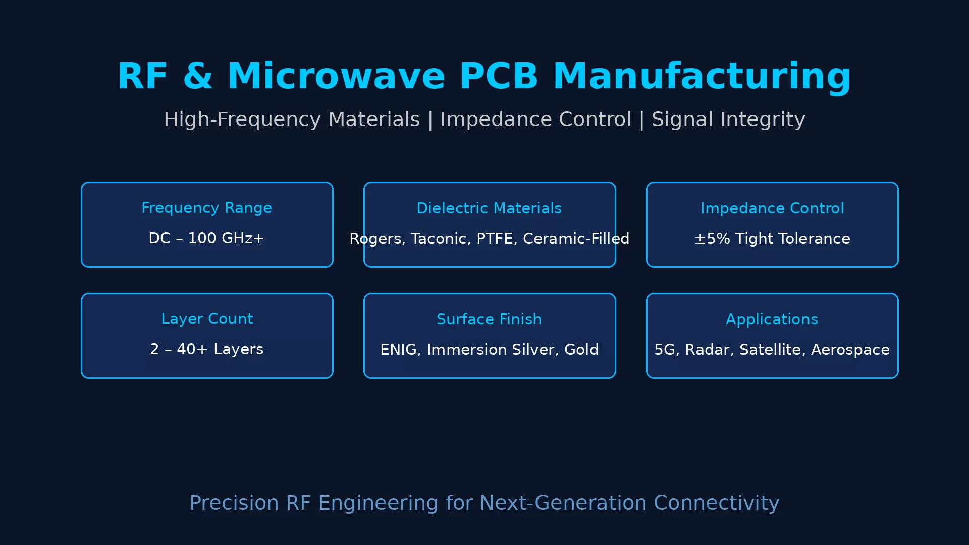
| Frequency Range | 500 MHz – 77 GHz (mmWave) |
| Min Line / Space | 0.05 / 0.05 mm (down to 0.035/0.035 mm in HDI fan-out zones) |
| Laminate Portfolio | Rogers RO4350B/RO4003C/RO4835; Taconic TLY-5/CER-10; PTFE/ceramic |
| Max Layer Count | Up to 68 (hybrid RF + digital), supports sequential lamination and HDI/ELIC |
| Layer Registration | ±0.025–0.06 mm — maintains coupling gaps and impedance stability |
| Impedance Control | ±5% mass production; special build to ±2% |
| Back-Drill Stub Control | Residual stub ≤ 0.25 mm (10 mil) — target ≤ 10 mil for RF links |
| Surface Finishes | ENIG, ENEPIG, Immersion Silver (preferred for antenna zones), OSP, selective hard gold |
| Via & Fill | Blind/buried via, resin plug, copper fill, VIP — reduces via inductance for RF BGAs |
| Test & Metrology | TDR impedance coupon every panel; flying probe full netlist; microsection QC |
| Min Drill (Mech. / Laser) | 0.15 mm / 0.075 mm |
| Board Thickness | 0.2 – 12 mm |
| Max Lamination Cycles | 7 (including sequential lamination) |
| Single-Ended Impedance | 50Ω |
| Back-Drill Depth Control | ±0.05 mm |
| Min Cavity / Step Width | 2.5 mm |
| Buried Resistor | 50Ω, ±10% |
Quality & Standards Compliance
RF and microwave PCBs are manufactured and inspected to IPC-6018 — the performance specification for high-frequency printed boards. Laminate selection follows IPC-4103 slash sheets for RF/microwave base materials. Verification includes TDR, controlled-impedance test coupons on every production panel, and microsection analysis for plated through-hole integrity in PTFE substrates.
Send your RF PCB requirements to pcba@superb-tech.com for material recommendation and quotation.





