


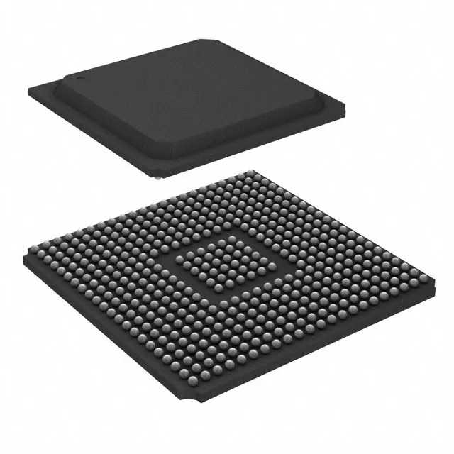

CVSS-945X-100.000
The CVSS-945X-100.000 is a 100MHz Voltage Controlled Crystal Oscillator (VCXO) from Crystek Corporation, delivering a True SineWave output with +5dBm drive into 50 ohms. Built on the CVSS-945 platform, this oscillator achieves a phase noise floor of -172.9 dBc/Hz at 1 MHz offset — corresponding to femtosecond-level integrated jitter. With 20ppm minimum APR pullability, sub-harmonic-free output, and a compact 9x14mm SMD package, it serves as a precision reference for PLL-based synthesizers, test equipment, radar systems, satcom transponders, and any application demanding ultra-low phase noise with voltage-controlled frequency adjustment.
Product Specifications
CVSS-945X-100.000 - Crystek VCXO 100MHz True SineWave Oscillator
Crystek Corporation - Voltage Controlled Crystal Oscillator, 100MHz, +5dBm SineWave, -172.9 dBc/Hz Noise Floor
MFR Part #: CVSS-945X-100.000Superb SKU: SUP-CVSS-945X-100.000
In Stock - Ready to Ship
The CVSS-945X-100.000 is a 100MHz Voltage Controlled Crystal Oscillator (VCXO) from Crystek Corporation, delivering a True SineWave output with +5dBm drive into 50 ohms. Built on the CVSS-945 platform, this oscillator achieves a phase noise floor of -172.9 dBc/Hz at 1 MHz offset — corresponding to femtosecond-level integrated jitter. With 20ppm minimum APR pullability, sub-harmonic-free output, and a compact 9x14mm SMD package, it serves as a precision reference for PLL-based synthesizers, test equipment, radar systems, satcom transponders, and any application demanding ultra-low phase noise with voltage-controlled frequency adjustment.
Request QuoteContact Sales
Key Performance Highlights
Output Frequency
100.000 MHz
Output Waveform
True SineWave
Output Level
+5 dBm into 50 ohm
Phase Noise Floor
-172.9 dBc/Hz
Pulling Range (APR)
20 ppm min
Package
9 x 14 mm SMD
Technical Specifications
| Manufacturer | Crystek Corporation |
| Part Number | CVSS-945X-100.000 |
| Product Series | CVSS-945 (High Frequency SineWave VCXO) |
| Device Type | Voltage Controlled Crystal Oscillator (VCXO) |
| Output Frequency | 100.000 MHz |
| Frequency Range (Series) | 50 MHz to 125 MHz |
| Output Waveform | True SineWave |
| Output Power | +5 dBm minimum into 50 ohms |
| Harmonic Suppression | < -25 dBc |
| Sub-Harmonics | None (sub-harmonic free design) |
| Phase Noise Floor | -172.9 dBc/Hz at 1 MHz offset |
| Jitter Performance | Femtosecond-level (ultra-low integrated RMS jitter) |
| APR Pullability | 20 ppm minimum (Absolute Pull Range) |
| Control Voltage Range | 0.5V to 4.5V (typical) |
| Supply Voltage | 5.0 V DC |
| Current Consumption | 30 mA max |
| Modulation Bandwidth | Typical VCXO modulation BW (kHz range) |
| Package | 9 mm x 14 mm SMD, 4-pad no-lead |
| Pin Configuration | VCC / GND / RF Out / VC (Control Voltage) |
| RoHS | RoHS Compliant |
Product Details
VCXO Design & Phase Noise
The CVSS-945 series from Crystek combines a high-Q crystal resonator with a low-noise oscillator circuit and voltage-controlled tuning element. The result is a True SineWave output with femtosecond-level integrated jitter — among the quietest commercially available VCXOs.
Phase Noise Floor: -172.9 dBc/Hz at 1 MHz offset. This ultra-low noise floor makes the CVSS-945X ideal as a reference oscillator in PLL-based frequency synthesizers where close-in phase noise is dominated by the reference, but far-out noise depends on the VCXO itself.
Sub-Harmonic Free: Unlike many VCXO designs that generate sub-harmonics (f/2, f/4, etc.), the CVSS-945X is sub-harmonic free — critical for direct-conversion receivers, frequency multiplier chains, and applications where spurious tones cannot be tolerated.
Key Applications
PLL Frequency Synthesizers - Ultra-low-noise reference for VCO/PLL loops
Test & Measurement - Spectrum analyzers, signal generators, phase noise analyzers
Telecom Infrastructure - Base station clocking, network synchronization (SyncE/IEEE 1588)
Radar Systems - Coherent LO generation, Doppler processing reference
Satellite Transponders - On-board frequency references, bent-pipe LO chains
Jitter Cleaning - VCXO-based jitter attenuator / clock recovery PLLs
High-Speed Data Converters - ADC/DAC sampling clock generation with fine frequency adjustment
VCXO vs XO vs TCXO Comparison
| Feature | VCXO (CVSS-945X) | XO (Fixed) | TCXO |
|---|---|---|---|
| Frequency Adjustment | Voltage-controlled (20ppm+) | Fixed (no adjustment) | Temperature-compensated (fixed) |
| Phase Noise | Excellent (-172.9 dBc/Hz floor) | Excellent (similar VCXO) | Good (compensation adds noise) |
| Primary Use | PLL locking / frequency margining | General clock generation | Temperature-stable reference |
| Output Type | True SineWave | CMOS/LVDS/HCSL/clipped sine | Clipped sine/CMOS |
| Temperature Stability | Standard (crystal-limited) | Standard (crystal-limited) | Excellent (compensated, sub-1ppm) |
| Harmonic Purity | < -25 dBc, no sub-harmonics | Good (depending on output type) | Moderate (clipped sine) |
Why Source CVSS-945X-100.000 from Superb Automation?
Frequency Reference BOM - VCXO + PLL IC + loop filter + buffer amplifier + PCB - one PO
Low-Noise PCB Design - Dedicated ground planes, guard rings, and power supply filtering for phase-noise-critical layouts
Impedance-Controlled Routing - 50-ohm microstrip lines for sine wave output with proper termination
VC Tuning Circuitry - Low-noise DAC + active filter for clean, glitch-free control voltage generation
25 Years Trusted - Electronic components + PCBA partner since 2000
Genuine Parts - Direct from authorized channels, full lot traceability
Frequently Asked Questions
What is the CVSS-945X-100.000 used for?
The CVSS-945X-100.000 is a 100MHz Voltage Controlled Crystal Oscillator used as a precision frequency reference in PLL synthesizers, test equipment, radar LO chains, telecom infrastructure, and satcom systems. Its voltage control input enables frequency locking, clock recovery, and jitter cleaning.
What is the phase noise performance?
The CVSS-945 series achieves a phase noise floor of -172.9 dBc/Hz at 1 MHz offset, with femtosecond-level integrated RMS jitter. This is among the best available for a commercial VCXO, making it suitable for high-purity signal generation applications.
What is the difference between VCXO and standard XO?
A VCXO adds voltage-controlled frequency tuning (20ppm min for CVSS-945X) to a crystal oscillator. Apply 0.5-4.5V to pull the frequency for PLL locking or clock synchronization. A standard XO outputs a fixed frequency with no tuning capability.
What output level does this VCXO provide?
True SineWave at +5 dBm minimum into 50 ohms (approximately 0.4 Vrms or 1.12 Vpp). Harmonics are below -25 dBc with no sub-harmonics. This clean output requires no external filtering for most applications.
How do I connect the CVSS-945X-100.000?
The 9x14mm SMD package has 4 pads: VCC (5.0V), GND, RF Output (50-ohm sine wave), and VC (control voltage 0.5-4.5V for frequency pulling). Route the RF output on a 50-ohm microstrip or coplanar waveguide trace. Use a low-noise voltage source for the control voltage input to preserve phase noise performance.
