

As 1.6T optical modules move from sampling to volume production, PCB technology has quietly become one of the biggest bottlenecks in the supply chain. The modified semi-additive process (mSAP), once a niche technique for high-end smartphones, is now mandatory for AI optical module PCBs. Here is what procurement teams, engineers, and EMS partners need to understand.
1. mSAP: From Apple Niche to AI Infrastructure Essential
For years, mSAP was known primarily as the PCB process behind high-end smartphone motherboards. The market was small, and few manufacturers invested in large-scale capacity.
That changed when 1.6T optical modules entered volume production. The signal integrity requirements of 224Gbps per channel cannot be met by traditional PCB processes. mSAP became a hard requirement — not a nice-to-have.
Google's hardware ecosystem now mandates mSAP for Co-op designs. NVIDIA's Rubin Ultra uses an 8+36+8 stack-up with mSAP on both outer layers. As 3.2T and NPO (Near-Package Optics) products mature, mSAP demand will only grow.
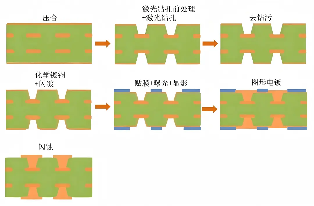
2. The 35-Micron Line: Where HDI Ends and mSAP Begins
The technical boundary is clear. HDI (High-Density Interconnect) handles trace widths from 35 to 90 microns reliably. Below 35 microns, HDI yields drop sharply. mSAP picks up at 35 microns and scales down to 10 microns.
At sub-35-micron line widths, mSAP yields are 8 to 10 percentage points higher than HDI. For 1.6T optical modules — high unit price, high performance requirements — yield and signal integrity matter more than marginal process cost savings. This is why mSAP is non-negotiable at 1.6T and beyond.
| HDI | mSAP | |
|---|---|---|
| Trace width range | 35–90 μm | 10–35 μm |
| 800G optical module | Viable | Preferred |
| 1.6T optical module | Insufficient | Required |
| 3.2T / NPO | Not viable | Mandatory |
| Cross-section shape | Trapezoidal (tapered sides) | Near-rectangular (vertical walls) |
| Signal loss | Higher (skin effect on tapered edges) | Lower (uniform cross-section) |
3. Why Trace Shape Matters: Subtractive vs. Semi-Additive
In traditional subtractive PCB fabrication, a full copper layer is laminated onto the substrate, then chemically etched away to leave the desired traces. The etching chemical attacks copper from all directions — downward, but also laterally from the sides, and gravity adds an extra taper. The result is a trapezoidal cross-section: wider at the top, narrower at the bottom.
At 224Gbps, that trapezoidal shape creates measurable signal loss. The uneven current distribution along the tapered edges increases impedance variation and attenuation.
mSAP flips the approach. Instead of starting with full copper and etching down, it starts with an ultra-thin chemical copper seed layer and electroplates copper upward only where traces are needed. The result is a near-vertical rectangular cross-section. Uniform thickness. Predictable impedance. Lower loss.
4. The mSAP Process Flow: Key Steps
Material prep: Ultra-thin copper foil (1/4 oz or carrier-type) from suppliers like Mitsui. Drilling and desmear follow.
Chemical copper deposition (seed layer): A very thin electroless copper layer is deposited on the entire substrate surface and hole walls. This seed layer is conductive but too brittle and thin to serve as final traces.
Dry film lamination, exposure, development: Similar to photoresist in semiconductor manufacturing. LDI (Laser Direct Imaging) opens windows where copper traces will be formed.
Pattern electroplating: Copper is electroplated into the open windows, building up to the required trace thickness. This is the actual circuit formation step — not etching.
Dry film stripping: The remaining photoresist is removed.
Flash etching: The thin seed layer and base copper foil between traces are rapidly etched away, leaving only the electroplated traces. Because the seed layer is extremely thin, flash etching is quick and minimally attacks the formed traces.
5. M8 Laminate and 16-Layer Stack-Up: The Real Cost Drivers
1.6T optical module PCBs are not simply "denser 800G PCBs." Two structural changes drive up cost significantly:
Material grade jump: 800G modules use M6 or M7 laminates. 1.6T modules require M8-grade laminates, which cost approximately 20.6% more than M6. Since March 2026, M8 prices have risen another 10%, with continued upward pressure through May.
Layer count increase: The common 1.6T PCB uses a 4+8+4 structure — 16 layers total. The middle 8 core layers can use HDI, while the outer 4+4 layers need mSAP for high-speed signal routing. Every additional layer means repeated lamination, drilling, plating, and imaging cycles — expanding production time and lowering throughput.
Price trajectory: 1.6T optical module PCB unit prices have moved from ~210–220 RMB in early 2026 to 280–290 RMB in February, then to 340–360 RMB. Target pricing of 420 RMB is within reach based on current supply tightness.
6. Supply Outlook: Tight Through September 2027
The mSAP capacity shortage is driven by equipment lead times, not lack of capital. Key bottlenecks:
Electroplating equipment: 15–18 month delivery cycle. Most manufacturers placed orders in February–March 2026, meaning new capacity arrives around September 2027.
Lamination presses: Similarly long lead times, with capacity further diluted by increasing layer counts.
Yield ramp: Even after equipment installation, mSAP requires months of process tuning — trace uniformity, via reliability, plating consistency, flash etch control, multi-layer registration.
Industry-wide, current mSAP capacity is approximately 1.4 million sqm/year, with planned expansion to 4.0–4.5 million sqm/year. But planned capacity is not effective capacity. Layer count increases alone reduce throughput by roughly 15% per additional layer.
7. mSAP Pricing: Optical Module Grade vs. Automotive Grade
| Application | Price (RMB/sqm) | Multiple |
|---|---|---|
| Automotive electronics mSAP | 3,000–4,000 | Baseline |
| General mSAP (2026 average) | 5,500–6,000 | ~1.5× |
| 1.6T optical module mSAP | 36,000–38,000 | ~10× vs. automotive |
The 10× premium reflects more than brand markup. Optical module mSAP demands tighter line-width tolerance, lower signal loss, higher layer reliability, and more complex stack-ups. It is a different product from generic mSAP — closer to IC substrate manufacturing than conventional PCB fabrication.
8. What This Means for Buyers: A Procurement Checklist
Line width capability: Can they reliably produce sub-35μm traces? Ask for cross-section micrographs, not just spec sheets.
M8 laminate supply: Do they have secured allocation of M8-grade CCL? Lead times for M8 are extending.
mSAP capacity allocation: What percentage of their mSAP line is dedicated to optical module PCBs vs. other products?
Yield data: What is their actual production yield at 25μm line/space? Below 85% is a red flag.
Equipment timeline: When is their next electroplating line arriving? When will it be qualified?
CCL and copper foil sourcing: Do they use Mitsui-grade ultra-thin copper foil or lower-tier alternatives?
Customer references: Have they shipped 1.6T optical module PCBs to any tier-1 optical transceiver manufacturer?
9. The Bigger Picture: PCB Value in AI Servers
mSAP is not just an optical module story. AI server PCBs are also transforming:
Vera Rubin configuration: ~3 million RMB in PCB value per rack, driven primarily by the orthogonal midplane.
Ultra Rubin with orthogonal backplane: PCB value estimated above 7 million RMB per rack.
GB300 (no orthogonal plane): Under 800,000 RMB in PCB value per rack — one-tenth of the Ultra Rubin figure.
Orthogonal backplanes remain in third-stage testing at all major manufacturers. A certification decision is expected in the coming months, but mass production still faces significant process challenges. This is a high-value direction, not a confirmed order book.
10. Our Take: What SUPERB Brings to the Table
As an EMS provider with deep PCB fabrication expertise, we track mSAP capacity, laminate pricing, and equipment lead times continuously. For customers developing 1.6T optical modules or AI server hardware, we offer:
Supplier matching: We know which PCB manufacturers have real mSAP capacity — not just marketing claims — and what their current lead times look like.
DFM review: Before you commit to a stack-up, we can flag manufacturability issues that would delay qualification or hurt yields.
Supply chain visibility: M8 laminate, ultra-thin copper foil, and high-end glass fabric are all constrained. We help you understand the real availability timeline.
Full EMS integration: From bare PCB to assembled and tested module, we handle the complete chain under one roof.
SUPERB Automation
www.superb-tech.com
July 2026
Adapted from industry analysis originally published June 2026. Source: sinovale.com





