HDI Manufacturing Parameters
| Max Layer Count | 30-layer ELIC (Every Layer Interconnect) |
| Max Production Size | 540 × 620 mm |
| Board Thickness Range | 0.20 – 4.0 mm |
| Min Core Thickness | 0.05 mm |
| Min Laser Hole / Pad | 0.05 mm / 0.15 mm |
| Min Mechanical Hole / Pad | 0.15 mm / 0.30 mm |
| Min Line Width / Spacing | 0.035 / 0.035 mm |
| BGA Pitch | 0.30 mm |
| Copper Thickness | 1 oz (standard) |
| Layer Registration | ±0.06 mm |
| Hole Filling Depression | ≤ 8 µm |
| Warpage | ≤ 0.5% |
| PTH Tolerance | ±0.075 mm |
| NPTH Tolerance | ±0.05 mm |
| Press-Fit Hole Tolerance | ±0.05 mm |
| Slot Hole Tolerance | ±0.10 mm |
| Outline Tolerance | ±0.10 mm |
HDI Build-Up Types
| Build-Up | Description | Typical Via Structure |
| 1-N-1 | One build-up layer on each side of the core. Entry-level HDI — suitable for moderate-density designs. | Blind micro-vias from L1→L2 and L(N)→L(N-1) |
| 2-N-2 | Two build-up layers on each side. Stacked or staggered micro-vias. Widely used in smartphones and automotive. | Stacked vias: L1→L2→L3; staggered offset for reliability |
| 3-N-3 | Three build-up layers per side. Higher routing density for advanced consumer and medical devices. | Stacked through all build-up layers |
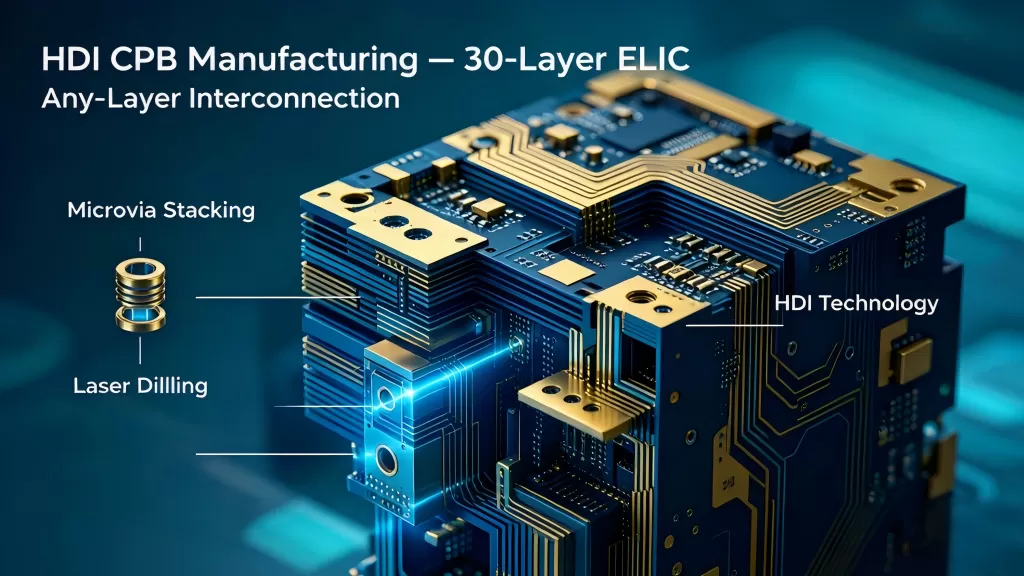
| Any-Layer (ELIC) | Every layer can connect to every other layer via stacked copper-filled micro-vias. Maximum density — flagship smartphones, AI modules, advanced semiconductor packaging. | Copper-filled stacked vias through all layers; sequential lamination |
HDI-Specific Manufacturing Processes
Laser Micro-Via Drilling
Focused UV laser energy ablates dielectric material to create 0.05 mm micro-vias with positional accuracy of ±0.025 mm. Laser vias stop on a copper target pad on the next layer below — this is essential for reliable via formation and is standard in every HDI build. The smooth, carbon-free via wall enables direct metallization without desmear processing.
Copper-Filled Via-in-Pad (VIP)
Via-in-pad with copper filling places the micro-via directly inside the BGA land pad — eliminating the dog-bone fanout and freeing significant routing space. Copper fill provides a flat, solderable surface on the pad while maintaining electrical connection to the inner layer. Hole filling depression is controlled to ≤ 8 µm for reliable BGA solder joint formation.
Sequential Lamination
Any-layer HDI (ELIC) is built through sequential lamination — fabricating the core, then adding build-up layers one pair at a time with repeated imaging, laser drilling, plating, and lamination cycles. Each cycle demands precise layer-to-layer registration (±0.06 mm) to ensure stacked micro-vias align correctly through the entire board thickness.
Solder Mask on Fine-Pitch BGAs
At 0.3 mm BGA pitch, solder mask dams between pads are measured in microns. LDI solder mask exposure with ±5% registration tolerance ensures dam integrity — preventing solder bridging between adjacent BGA balls during reflow.
HDI Applications
| AI & GPU Modules | AI accelerator subsystems, GPU carrier boards, chiplet interconnect substrates — 0.3mm BGA, ELIC stackup |
| Automotive ADAS | Camera modules, radar sensor processors, domain controllers — 2-N-2 or 3-N-3, staggered vias for reliability |
| Smartphones & Wearables | Flagship phone mainboards, smartwatch system boards — any-layer ELIC, 0.035mm line, ultra-thin cores |
| Communication Devices | 5G mmWave antenna-in-package substrates, RF front-end modules, small-cell baseband processors |
| Medical Implants | Implantable device substrates, hearing aid modules — ultra-thin, high-reliability, biocompatible materials |
| Advanced Packaging | IC substrates, interposers, fan-out wafer-level packaging — finest line/space and laser via capability |
Send your HDI PCB requirements to pcba@superb-tech.com for a free DFM review and quotation.