


20L Hybrid PCB — PTFE+FR4, Embedded R, Blind | Superb Automation
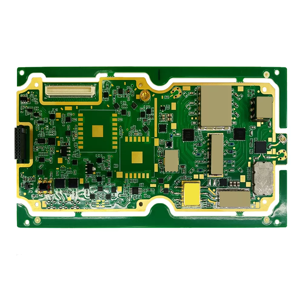
Hybrid PCB manufacturing — PTFE+FR4 · 20 layers · 5.7 mm · 4-step blind via · Blind slot · Embedded resistors · Back drill · Build-to-print from Gerber files
Product Specifications
Hybrid / Mixed-Material PCB Fabrication
Hybrid PCB manufacturing — PTFE+FR4 · 20 layers · 5.7 mm · 4-step blind via · Blind slot · Embedded resistors · Back drill · Build-to-print from Gerber files
Capabilities
| Layer count | 20 layers (PTFE + FR-4 mixed lamination · Single-press) |
| Finished board thickness | 5.7 mm |
| Materials | PTFE (Rogers / Taconic) + FR-4 (high-Tg) |
| Blind via | 4-step blind via · Blind slot · Multiple blind/buried via sequences |
| Back drill | Blind via back drill · Through-hole back drill · Stub control |
| Embedded resistors | Multi-level inner-layer embedded resistors · 8 resistance values |
| Half-hole | Controlled-depth half-hole (castellated) |
| Step features | Surface finish, trace, solder mask, silkscreen inside steps |
| Surface finish | ENIG · ENEPIG · Immersion silver · Immersion tin · HASL lead-free · Hard gold |
| Impedance control | ± 5% differential (TDR verified per panel) |
| Max panel size | 610 mm × 480 mm |
Hybrid Lamination Process
Mixed-Material Single-Press
- Multiple materials (PTFE, ceramic-filled, FR-4) laminated in a single press cycle
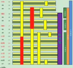
- Material stack-up design with CTE matching across dissimilar substrates
- Dk range from 2.2 (PTFE) to 4.5 (FR-4) on the same board
- Bonding film selection: Rogers 3001, Speedboard C, FR-4 prepreg by zone
4-Step Blind Via
- Sequential build-up: four lamination + drill + plate cycles
- Laser-drilled microvias through PTFE layers — plasma desmear activation
- Stacked and staggered via configurations across all four steps
- Copper-filled blind vias (via-in-pad) for high-density BGA routing
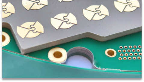
Blind Slot
- Slot routed to controlled depth, stopping on a copper plane
- Slot sidewall plated — copper continuity to inner layers
- Used for RF cavity integration, waveguide coupling, and mechanical interlock
Embedded Resistors
- Multi-level inner-layer planar resistors: 8 discrete resistance values
- OhmegaPly® or Ticer® thin-film resistor foil, patterned with trace layers
- Laser trim to ± 5% tolerance per resistor value
- Eliminates discrete SMD resistors — saves board area, improves reliability
Back Drill
- Blind via back drill — removes unused via stub in blind hole stack
- Through-hole back drill — stub length controlled to < 0.25 mm
- Depth-controlled drilling with conductive inner-layer target pad
Step Features
- Milled steps with internal surface finish, trace routing, solder mask, and silkscreen
- Multiple step heights on a single board — 3D topography for connector mating and heatsink seating
Applications
- Phased-array antenna — RF beamforming on PTFE + digital beam-control on FR-4 · One board
- Aerospace transceiver — Ku/Ka-band front-end + IF/baseband in a single hybrid stack
- 5G base station filter — cavity filter integrated into PCB via blind slot + step
- Satellite payload — low-Dk PTFE for LNA + FR-4 for power distribution
- Defense electronics — mixed-signal, high-reliability, single-board LRU replacement
- Medical imaging — ultrasound front-end (PTFE) + digital back-end (FR-4) hybrid
Why Hybrid Lamination
- One board replaces two or more assembled PCBs — eliminates inter-board connectors and cables
- RF and digital circuits on a single substrate — reduced latency, improved phase coherence
- Each zone uses the optimal material — low-Dk PTFE for RF, cost-effective FR-4 for digital
- Fewer mechanical interfaces — better vibration and thermal cycling reliability
- Single DFM review, single fabrication run — shorter lead time than multiple boards
Gerber file review & DFM → pcba@superb-tech.com
Superb Automation Co., Limited · Hybrid PCB Manufacturing · Wuxi + Huizhou