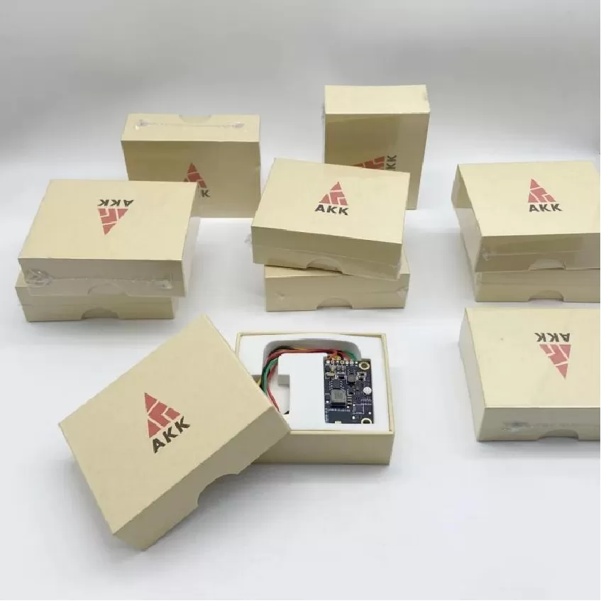
UAV Signal Processing Board PCBA
UAV Signal Processing Board PCBA. UAV Avionics PCBA, Flight Control Board, FPV Transmitter, Navigation Fusion, Mission Control, Video Transmission, DO-254,
Product Specifications
UAV Signal Processing Board PCBA
16-Channel Simultaneous-Sampling Analog Front-End with Onboard DSP
Product Overview
The UAV Signal Processing Board is a multi-channel analog and digital signal conditioning PCBA that serves as the sensory nervous system of advanced unmanned aerial platforms. Modern UAVs carry a diverse array of sensors — analog transducers for temperature, pressure, and vibration; digital I²C and SPI environmental sensors; LIDAR rangefinders outputting PWM or analog voltage; and ultrasonic sensors requiring high-frequency pulse generation and echo detection. This board consolidates all sensor interface and conditioning functions onto a single PCBA, providing clean, calibrated, timestamped data to the flight controller or mission computer through a unified digital interface, eliminating the wiring complexity and noise susceptibility of distributed sensor wiring.
The 6-layer PCB features a fully differential analog front-end with 16 simultaneously sampled channels at 24-bit resolution. Each channel includes a programmable gain instrumentation amplifier, an anti-aliasing low-pass filter with software-selectable cutoff frequency, and a precision voltage reference with 5 ppm/°C temperature drift. All analog signal paths are routed over an unbroken ground plane and shielded by guard traces driven to the common-mode voltage, achieving >100 dB of channel-to-channel crosstalk isolation. An onboard STM32H7 microcontroller performs real-time digital filtering (FIR, IIR, and Kalman), linearization of nonlinear sensor responses, and timestamping of all samples against a GPS-disciplined 1PPS signal, enabling precise temporal correlation with other subsystems. The board also generates excitation voltages and currents for bridge sensors, thermocouples, and RTDs.
Key Specifications
| Channels | 16 differential, simultaneous sampling |
| ADC Resolution | 24-bit, 200 kSPS per channel |
| Crosstalk Isolation | >100 dB channel-to-channel |
| Voltage Reference | 5 ppm/°C drift, precision |
| Sensor Excitation | Bridge, thermocouple, RTD outputs |
| Onboard Processing | FIR, IIR, Kalman filtering (STM32H7) |
| Timestamp Accuracy | GPS 1PPS, ±1 µs |
| Digital Output | CAN-FD, SPI, UART |
PCBA Assembly Challenges
Assembling a precision analog front-end demands meticulous SMT process control to preserve the low-noise characteristics of the design. The 24-bit ADC and instrumentation amplifiers are sensitive to flux residues, which can create parasitic leakage paths on the order of nanoamps — enough to introduce several LSBs of offset error. All analog components are assembled using no-clean flux with post-reflow aqueous cleaning to achieve surface insulation resistance exceeding 10¹² Ω. The precision voltage reference (5 ppm/°C) requires placement in a low-thermal-gradient region of the board, away from the STM32H7 processor and voltage regulators. Guard traces are verified for continuity and correct common-mode drive voltage after assembly using a precision source-measure unit. Thermocouple cold-junction compensation accuracy depends on the isothermal layout of the input connector and reference sensor; both are co-located on a dedicated copper island thermally isolated from the rest of the board.
Test Strategy
Each assembled signal processing board undergoes a rigorous analog validation sequence. All 16 channels are simultaneously stimulated with a precision voltage source swept across the full input range, and gain error, offset error, INL, and DNL are measured at multiple temperatures (-40°C to +85°C). Crosstalk is verified by driving a full-scale sine wave on one channel and measuring the induced signal on all adjacent channels. The excitation outputs are loaded to rated current and validated for voltage accuracy and noise. Digital filtering algorithms are verified by injecting known waveforms (sine, square, triangle) and comparing the filtered output against a MATLAB golden reference. GPS timestamp accuracy is validated using a GPS simulator providing a known 1PPS reference. A NIST-traceable calibration report is generated for every board across the full operating temperature range.
PCB Manufacturing Difficulty
Fabricating the bare PCB requires careful management of mixed-signal design rules. The 6-layer stack-up dedicates two internal layers to unbroken ground planes — one for analog and one for digital — connected at a single star point beneath the ADC to prevent ground loops. The analog guard ring traces are routed at 6 mil width with tight tolerance to maintain consistent impedance. The board uses FR-4 with a Tg of 170°C, selected for dimensional stability during multiple reflow cycles. Controlled impedance is specified for all differential digital pairs (CAN, SPI) at 120 Ω, verified by TDR on impedance coupons at the panel edge. The minimum drill size of 0.25 mm is used for all vias in analog signal paths to minimize via inductance and its effect on high-frequency noise coupling.
More information