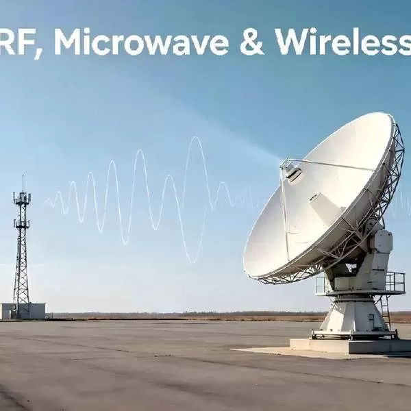
RF and microwave PCB design operates under physics that commercial digital boards never encounter. At frequencies above 1 GHz, every trace is a transmission line, every via is an inductor, and every plane gap is an antenna. A phased-array radar board at 30 GHz has wavelengths of approximately 5mm in Rogers 4350B — meaning a 1mm trace length mismatch between two channels creates a 72° phase error. Tolerance stacking at these frequencies leaves zero room for manufacturing variation.
Material selection is the single most consequential decision in RF PCB design. Standard FR-4 has a dissipation factor (Df) of ~0.020 at 10 GHz — completely unusable for most RF applications. RF laminates like Rogers 4350B (Df=0.0037), Rogers 4003C (Df=0.0027), and PTFE-based materials are mandatory. Hybrid stackups combining RF laminates on outer layers with FR-4 cores offer a cost-optimized path for mixed-signal designs where only the RF section demands low-loss materials.
Testing RF boards requires fundamentally different equipment than digital boards. Vector network analyzers (VNAs) measure S-parameters across frequency sweeps to verify impedance matching, insertion loss, and isolation. A single poorly tuned antenna feed network can cost 3-6 dB of gain — the equivalent of halving the effective transmit power.
Our RF & Microwave PCB Solutions
Proven Capabilities
Superb Automation produces RF and microwave PCBs for defense, aerospace, telecommunications, and SATCOM applications. Our RF manufacturing line is optimized for the unique demands of high-frequency design:
| Requirement | Industry Standard | Superb Capability |
|---|---|---|
| Layer Count | 2-12 layers | 2-24 layers, including hybrid RF/digital stackups |
| RF Laminates | Rogers 4350B, 4003C | Rogers 4350B, 4003C, 3003, RT/duroid 5880, 6002, Taconic, Isola Astra |
| Max Frequency | Up to 20 GHz | Verified to 40 GHz; 77 GHz mmWave on request |
| Impedance Control | ±10% | ±7% standard; ±5% for critical RF paths |
| Surface Finish | ENIG | ENIG, ENEPIG, immersion Ag, selective hard gold (RF connectors) |
| Special Processes | Mixed dielectric | Cavity PCB, edge plating, hybrid stackup, blind/buried vias, metal-backed PCB |
| Testing | AOI, flying probe | AOI, flying probe, VNA (4-port S-parameter), TDR, spectrum analysis |
| Certifications | IPC Class 2 | IPC-A-610 Class 3, IPC-6012 Class 3, ISO 9001, MIL-PRF-31032 ready |
Application Examples
Phased-Array Antenna Boards
Multi-element beamforming arrays with phase-matched feed networks, Wilkinson dividers, and integrated TR modules. Typical: 6-16 layers, Rogers 4350B/4003C, ±5% impedance control.
SATCOM Up/Down Converters
Ka/Ku-band frequency conversion boards with mixers, LO chains, and IF filtering. Typical: 6-12 layers, Rogers 4003C, cavity shielding, low PIM finish.
Radar Front-End Modules
FMCW/pulse radar transceiver boards with integrated PLL/VCO, LNA, PA, and baseband processing. Typical: 4-10 layers, Rogers 4350B, thermal management for PA stages.
5G mmWave Antenna-in-Package
28/39 GHz AiP boards for 5G FR2 small cells and CPE with integrated patch arrays and beamforming ICs. Typical: 8-14 layers, Megtron 7 + Rogers hybrid, advanced HDI.
RF Filter & Diplexer Boards
Stripline/microstrip filter boards with precise resonator geometries for L, S, C, and X-band. Hairpin, interdigital, and combline topologies. Typical: 2-6 layers, low-Dk stable laminates.
RF Test & Calibration Fixtures
Precision calibration standards and test fixture boards with characterized thru, reflect, and line (TRL) structures for VNA calibration. Typical: 2-4 layers, Rogers 4350B, tight Dk control.
PCB Types in This Industry — Technical Deep Dives
Explore detailed technical articles on the specific PCB types used in this industry:
RF Frontend Transceiver PCB — RF transceiver front-end PCBs for communication and radar.
RF Filtering, Matching & Impedance PCB — RF filtering, matching networks, and impedance control.
RF Signal Distribution & Switching PCB — RF signal routing, switching matrices, and distribution networks.
Phased-Array Beamforming Antenna PCB — Active electronically scanned array and beamforming antenna PCBs.
RF Test & Calibration PCB — RF test fixtures, calibration standards, and verification boards.
High-Frequency System Integration PCB — System-level RF integration, packaging, and interconnect.
More Industries We Serve
High-speed PCBs for GPU accelerators, edge inference modules, and AI vision systems with 100G+ signal integrity.
Server motherboards, switch line cards, and storage backplanes for hyperscale and enterprise data centers.
AEC-Q qualified PCBs for BMS, OBC, DC-DC converters, ADAS sensors, and in-vehicle networking.
Rugged PCBs for PLCs, motor drives, remote I/O, and industrial IoT — built for harsh factory environments.
High-frequency PCBs for 5G base stations, optical transport, core routers, and network security appliances.
Compact, low-power PCBs for smart sensors, wearables, smart home gateways, and battery-operated IoT endpoints.
ISO 13485 compliant PCBs for diagnostic imaging, patient monitoring, surgical instruments, and wearable health devices.
Avionics, satellite communication, radar signal processing, and military-grade PCBs — coming soon.
Solar inverters, wind turbine controllers, energy storage BMS, and grid infrastructure — coming soon.
Need a quote for your PCB project?
Info@superb-tech.com