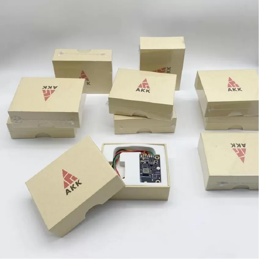
Power Management Board PCBA
Power Management Board PCBA. UAV Avionics PCBA, Flight Control Board, FPV Transmitter, Navigation Fusion, Mission Control, Video Transmission, DO-254, DO-1
Product Specifications
Power Management Board PCBA
Multi-Rail Power Distribution — 60 A Continuous, Redundant Critical Rails, Per-Rail Telemetry
Product Overview
The Power Management Board is the electrical lifeline of the UAV — a sophisticated multi-rail power conversion and distribution PCBA that takes raw battery voltage (typically 3S to 12S LiPo, 11.1 V to 50.4 V) and generates all the precisely regulated voltage rails required by the UAV's diverse avionics subsystems. A typical UAV requires 5 V for servos and RC receivers, 3.3 V for flight controllers and microcontrollers, 1.8 V and 1.2 V for FPGA and SoC core supplies, 12 V for cameras and gimbals, and potentially 24 V or 48 V for payloads. This board generates all these rails with high efficiency, low noise, and — critically — fault tolerance that prevents a single point of failure from bringing down the entire aircraft.
The 6-layer PCB uses 3 oz copper on the inner power planes to handle continuous currents up to 60 A with minimal I²R losses and temperature rise. Nine independent switching regulators based on Texas Instruments TPS546x and LMR series converters provide the main power rails, each with over-current, over-temperature, and under-voltage lockout protection. Critical rails (3.3 V and 5 V) are redundantly generated from two independent converters with OR-ing diodes, so a single regulator failure does not cause system loss. Ultra-low-noise linear post-regulators (LT3045, 0.8 µV RMS noise) supply the analog sensor rails, while dedicated LDOs power the RF sections with >60 dB of power supply ripple rejection. An onboard INA226 current/voltage monitor IC on each rail provides real-time telemetry to the flight controller over I²C, enabling per-rail power budgeting and early warning of anomalous current draw. The board also includes a battery fuel gauge with coulomb counting and a cell-balancing input for LiPo packs.
Key Specifications
| Input Voltage | 11.1–50.4 V (3S–12S LiPo) |
| Maximum Current | 60 A continuous |
| Output Rails | 9 regulated, 2 redundant |
| Efficiency | >92% at rated load |
| Analog Noise | <1 µV RMS (LT3045 post-regulator) |
| Telemetry | Per-rail V/I (INA226), I²C |
| Protection | OCP, OTP, UVLO on all rails |
| PCB | 6-layer, 3 oz inner copper |
PCBA Assembly Challenges
Assembling a high-current power distribution board presents challenges centered on thermal management and high-current interconnects. The 3 oz inner copper layers and 2 oz outer layers act as massive heat sinks during reflow, requiring extended soak times and higher peak temperatures to achieve full liquidus on all solder joints. The large switching inductors (often 10 × 10 mm or larger) and MOSFET packages have significant thermal mass; the reflow profile must hold above 217°C for 90–120 seconds to ensure complete wetting. The OR-ing diodes for the redundant rails are typically in DPAK or PowerDI packages that require void-free solder joints for thermal dissipation — X-ray inspection verifies void rates below 15% on these power components. The INA226 current-sense amplifiers rely on precision shunt resistors (typically 1 mΩ, ±1%) placed in the high-current path; Kelvin (four-terminal) connections from the shunt to the INA226 must be routed as differential pairs to reject common-mode noise. All high-current traces and power planes are verified post-assembly for resistance using a four-wire milliohm meter; any increase beyond the design value indicates poor solder joint quality.
Test Strategy
Each assembled Power Management Board undergoes full-load testing on every rail. A programmable electronic load applies the rated continuous current to each rail while a data acquisition system monitors output voltage, ripple, and efficiency. All rails are simultaneously loaded to 100% of rated capacity for 1 hour while thermal imaging verifies that no component exceeds its rated junction temperature. The redundant 3.3 V and 5 V rails are tested by deliberately disabling one converter and verifying that the OR-ing diode seamlessly transfers the load to the backup converter with less than 100 mV of transient droop. Protection circuits are tested by inducing over-current (electronically forcing the rail beyond its current limit) and verifying that the converter enters hiccup-mode protection; over-temperature is tested by locally heating the converter with a hot-air source. The INA226 telemetry channels are calibrated against a precision 6.5-digit DMM across the full current range. The battery fuel gauge is calibrated with a known discharge cycle. Every rail's noise spectrum is measured from 10 Hz to 1 MHz using a spectrum analyzer.
PCB Manufacturing Difficulty
Fabricating the 6-layer power board requires heavy-copper PCB processing capabilities. The inner power planes use 3 oz (105 µm) copper, which demands longer etch times and larger etch compensation factors to achieve the designed trace widths. The minimum trace/space on the 3 oz layers is 10/10 mil — finer geometries are not achievable with heavy copper. Plated through-holes for high-current paths (battery input, main rail outputs) are specified at 1.0 mm minimum diameter with 35 µm minimum copper wall thickness to handle the current density. The board material is a high-Tg FR-4 (Tg 170°C) to withstand the elevated operating temperatures associated with high-current operation. The outer layers use 2 oz copper with ENIG surface finish for the fine-pitch ICs. All inner layer clearances around plated through-holes are increased by 50% over standard designs to ensure adequate high-voltage creepage distances for the 50.4 V input. Finished boards undergo 100% high-pot (hipot) testing at 500 VDC between the input rail and ground to verify isolation integrity before assembly.
More information