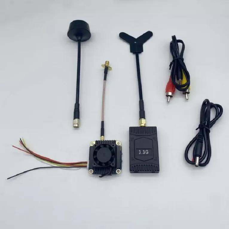
Beamforming Control Board PCBA
Beamforming Control Board PCBA. RF PCBA, Power Amplifier, LNA, RF Front-End, Phased Array, Beamforming, Antenna Array, Frequency Synthesizer, Rogers PCB, V
Product Specifications
Beamforming Control Board PCBA
Multi-Beam Digital Beamforming Engine — 16 Independent Beams, 500 MHz Instantaneous BW, 2.3–4.2 GHz
Product Overview
The Beamforming Control Board PCBA implements a multi-beam digital beamforming engine capable of simultaneously forming and steering up to 16 independent beams from a single antenna aperture across 2.3–4.2 GHz. The board digitizes each array element signal using synchronized multi-channel ADCs, then applies complex beamforming weights in an onboard FPGA fabric to synthesize multiple concurrent beam patterns. An ultra-low-skew clock distribution network — using matched-length differential lines with sub-picosecond accuracy — ensures coherent sampling across all channels, preserving the phase relationships essential for accurate beamforming. The high-speed JESD204C serial interface between ADCs and FPGA minimizes IO count while supporting the aggregate data bandwidth of 128 simultaneous channels. Onboard DDR4 memory stores multiple beam weight tables for instantaneous beam switching. Custom interposer connectors enable direct mounting to the antenna element board, eliminating cable-induced phase errors. This PCBA is the digital heart of advanced 5G massive MIMO base stations, SATCOM multi-beam gateways, and military digital array radar systems.
Key Specifications
| PCB Type | Beamforming Control Board |
| Frequency Range | 2.3–4.2 GHz |
| Independent Beams | 16 simultaneous |
| Instantaneous BW | 500 MHz |
| Material | Megtron 6 / Isola Astra |
| Layer Count | 14–22 layers, HDI blind vias |
PCBA Assembly Challenges
Assembling a digital beamforming board at this channel density presents one of the most demanding SMT challenges in RF PCBA. The board hosts a large FPGA with 2,500+ BGA balls alongside multiple multi-channel ADC ICs — all requiring precise placement with coplanarity within 0.1 mm to ensure reliable soldering. The high-speed JESD204C serial links between ADCs and FPGA operate at 12.5 Gbps per lane, demanding that every differential pair maintain strict impedance control and intra-pair skew below 1 ps through the assembly process. A single solder defect on a JESD204C lane can corrupt an entire bank of digital beamforming channels. The interposer connector array that mates with the antenna board requires exceptional flatness — the board is assembled on a precision fixture that holds connector alignment within ±3 mil across the full connector field. Mixed-technology assembly must manage the thermal mass mismatch between the large FPGA BGA and small passive 0201 components on the same board; a multi-zone reflow profile with extended soak time ensures all joints reach proper wetting. Post-reflow, every JESD204C lane is tested for eye diagram compliance, and X-ray inspection verifies BGA void rates below 15% on all FPGA and ADC packages.
Test Strategy
The Beamforming Control Board undergoes a multi-stage test sequence that validates both the high-speed digital fabric and the beamforming signal processing integrity. Flying probe ICT verifies all passive components and power rail impedances, with particular attention to the multiple low-noise analog supply rails feeding the ADCs. Boundary scan (JTAG) tests interconnects between the FPGA, DDR4 memory, and ADC SPI control interfaces. The clock distribution network is characterized by injecting a reference clock and measuring the phase offset at every ADC clock input using a multi-channel oscilloscope — any channel-to-channel skew exceeding 1 ps triggers rework. The JESD204C links are tested with a built-in PRBS pattern generator and checker, confirming error-free operation at 12.5 Gbps across all lanes. Beamforming functional testing loads the FPGA with a diagnostic beamforming firmware and injects a known RF test signal at the ADC inputs; the formed beam outputs are captured and compared against golden reference patterns for all 16 simultaneous beams. Thermal chamber testing from -40°C to +85°C verifies that the beamforming weights remain accurate and that no timing violations emerge on the JESD204C links under temperature extremes. Final system-level testing integrates the board with the antenna aperture for full far-field beam pattern verification.
PCB Manufacturing Difficulty
Manufacturing the bare PCB for a digital beamforming board requires world-class HDI capabilities. The 14–22 layer stackup uses sequential lamination with laser-drilled microvias for layer transitions in the dense FPGA and ADC breakout regions, with via-in-pad construction on the 0.8 mm pitch BGA sites to maximize routing density. Signal integrity is paramount: every JESD204C differential pair is modeled in 3D EM simulation for insertion loss, return loss, and crosstalk, with the fabricated board verified against the model using VNA measurements. The ultra-low-skew clock tree requires that all clock distribution traces be length-matched to within ±2 mil, with symmetric layer transitions to maintain phase balance. Low-profile copper foil (HVLP) is used on all high-speed signal layers to minimize conductor roughness losses at 12.5 Gbps. Backdrilling removes via stubs on all signal layers carrying JESD204C traffic. Impedance is controlled to 100 Ω ±8% on differential pairs and verified by TDR on panel test coupons. The finished board undergoes 100% AOI and flying probe netlist verification before being released to the assembly line.
More information