

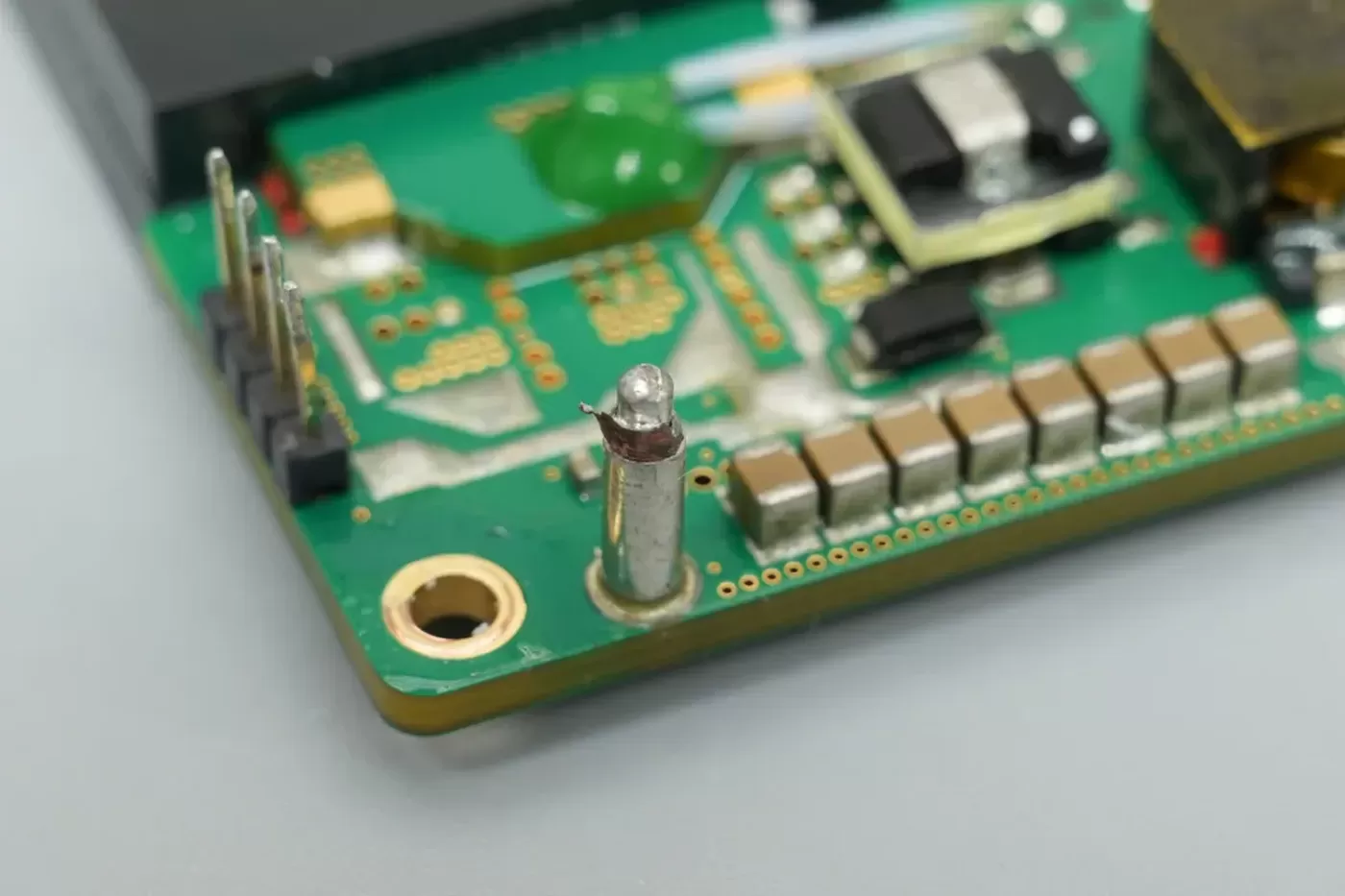
48V to 12V 800W Isolated DC-DC Brick Converter PCBA


Product Specifications
Product Overview
The 800 W brick is the standard power block behind a -48 V telecom bus. Input spans -38 V to -75 V, output is 12.2 V at 65.6 A, and the whole converter sits in an 85.97 x 60.14 x 10.4 mm package weighing 109 g. That package holds about 53.8 cm³, so the power density is roughly 14.9 W/cm³. Every watt has to leave through the baseplate and the pins, which is why the assembly, not the schematic, decides whether the module survives a 55 °C ambient at full load.
The topology is a full bridge on the primary with synchronous rectification on the secondary. A Renesas ISL6741 peak current mode controller runs the bridge at up to 2 MHz, driving TI UCC27201 half-bridge gates on the high side and UCC27423 low-side drivers on the synchronous rectifiers. Primary switches are Infineon BSC070N10NS3G, 100 V, 7 mΩ. Secondary rectifiers are onsemi FDMS86201, 120 V, 11.5 mΩ. Both sides parallel several devices to spread conduction loss, and the planar transformer carries the isolation and the turns ratio in its own PCB windings. Feedback crosses the barrier through a Renesas PS8101 optocoupler rated 3750 Vrms at 1 Mbps.
Mechanically the module is a heat-sink problem with a board attached. A thermal interface material sits between the module and the finned heatsink, the heatsink is screwed down, and the module only reaches rated power under forced air. Current sense transformers, an NTC on the transformer body, and the input and output posts are all part of the assembly, and each one has a soldering and placement tolerance that shows up as loss or as a hot spot.
Key Specifications
| Input Voltage | -38 V to -75 VDC, telecom -48 V nominal |
|---|---|
| Output | 12.2 V / 65.6 A |
| Rated Power | 800 W |
| Topology | Full bridge primary, secondary synchronous rectification |
| Controller | Renesas ISL6741, peak current mode, switching up to 2 MHz |
| Gate Drive | TI UCC27201 half bridge, TI UCC27423 low side |
| Primary Switches | Infineon BSC070N10NS3G, 100 V, 7 mΩ, TDSON-8 |
| Synchronous Rectifiers | onsemi FDMS86201, 120 V, 11.5 mΩ, Power 56 |
| Isolation Feedback | Renesas PS8101 optocoupler, 3750 Vrms, 1 Mbps |
| Dimensions | 85.97 x 60.14 x 10.4 mm |
| Weight | 109 g |
| Power Density | Approximately 14.9 W/cm³ |
| Cooling | Forced air with external heatsink and thermal interface |
| Assembly Standard | IPC-6012 Class 3, IPC-A-610 Class 3 |
PCBA Assembly Challenges
Parallel MOSFET current sharing. Four or more devices share the primary current and the same number share the secondary. Sharing is set by gate loop inductance, source inductance and Rds(on) spread, not by the schematic. A 3 nH difference in the source return of one device is enough to push disproportionate current into its neighbour at 800 W. We keep gate and source returns symmetric per device, verify loop length in DFM, and check joint voiding under every power package on X-ray before the board is released.
Planar transformer terminations. The transformer windings are PCB layers, so the interlayer registration, via stitching and the solder joint at each termination carry the full primary and secondary current. A void at one termination raises local temperature and shows up later as insulation breakdown. Terminations are reflowed with a dedicated profile and inspected by cross-section on first article.
Thermal path consistency. The module only meets its rating when the baseplate sits flat on the thermal interface. Solder mask thickness variation, via tenting and board warp all change the contact gap. We hold flatness on the thermal area, keep the interface area free of mask and silkscreen, and control screw torque during heatsink assembly so the gap stays even across the baseplate.
Heavy copper joints. Power layers run at 2 oz and above to carry 65 A. Thick copper wicks heat away from the joint during reflow, so the paste volume and soak time have to be raised or the joint stays cold. Input and output posts are through-hole and need full barrel fill, verified by X-ray on every panel.
Isolation barrier discipline. The optocoupler and the transformer both cross the barrier, and creepage has to survive 3750 Vrms. Solder balls, flux residue and mask skips near the barrier are the usual failure path. Barrier areas are kept clear of test points and get a dedicated visual and hi-pot check.
Mixed-technology reflow. The same board carries 0402 passives, fine-pitch control ICs and large power packages with different thermal mass. A single profile cannot keep both ends in spec, so the profile is set by the heaviest joint and the small parts are protected by soak time rather than by peak temperature.
Test Strategy
In-circuit test. All nets are probed for opens, shorts and value before power is applied. The gate drive resistors, current sense windings and the optocoupler pins are the first things a bad reflow takes out, and ICT catches them without powering the bridge.
X-ray and AOI. AOI covers placement and polarity. X-ray covers the power packages, the posts and the transformer terminations, with a void limit agreed with the customer on first article. Anything above the limit is reworked or scrapped, not shipped.
DC functional test. Input is ramped across the -38 V to -75 V range, output regulation, ripple, current limit, over-voltage and over-temperature protection are checked under electronic load. This is done on our line with our own fixtures.
Isolation test. Hi-pot is applied across the barrier at the rated voltage for the customer-specified dwell time, with leakage recorded per unit.
Efficiency and thermal verification. Efficiency curves and case temperature rise are measured with the customer fixture or at a third-party lab. We do not claim an in-house power analyser or thermal chamber for this class of module.
Burn-in. Not offered in house. Where the customer requires burn-in, it is written into the purchase order as a third-party step with the profile attached, not assumed.
PCB Manufacturing Difficulty
Heavy copper etching and plating. Power layers at 2 oz and above etch with a wider trace/space window and need tighter plating uniformity. Thin plating on a 65 A layer is a hot spot waiting to happen, so copper thickness is checked on coupons per panel.
Via and thermal management. Thermal vias under the power packages have to be filled and capped, otherwise solder wicks into the barrel and starves the joint. Via fill, planarisation and mask over the filled area are all process steps, not layout details.
Flatness for the heatsink interface. The module base has to sit on the thermal interface without rocking. Warp is controlled at lamination and checked after reflow, because reflow is where a flat panel becomes a curved board.
Registration across many layers. The planar transformer uses several layers in series, so layer-to-layer registration directly changes turns geometry and leakage inductance. Registration is held at the tighter end of the capability and checked on the first panel of each lot.
Routing and separation. Primary and secondary sit millimetres apart in a 10.4 mm tall package. Slot routing, creepage distance and the barrier keep-out are fixed at the panel stage, and the profile has to leave no burr on the isolation slot.
Applications
Telecom -48 V base station power. BBU and RRU shelves that run from a -48 V battery bus and need a regulated 12 V rail for digital cards.
Server and storage 12 V intermediate bus. Rack equipment that converts the facility or battery bus down to a 12 V intermediate rail feeding point of load converters.
O-RAN and D-RAN remote radio sites. Outdoor radio cabinets where the brick sits behind a fan tray and has to hold 800 W across a wide input range.
Edge data centre power shelves. Compact 1U shelves that stack several bricks in parallel and need matched modules, not just working ones.
Industrial 48 V DC systems. Telecom-derived 48 V rails in factory automation, testing racks and rail signalling equipment.
Test and measurement chassis. Instrument mainframes that need a quiet, isolated 12 V rail with predictable ripple at full load.
Why Superb Automation
- We source the controller, the gate drivers, the power MOSFETs and the planar transformer cores as one bill of materials, including the long lead time parts, so a single shortage does not stop the build.
- Heavy copper PCB fabrication, via fill and slot routing are handled in the same flow as the assembly, which keeps the thermal and isolation features from being designed out by the fabricator.
- SMT runs 0201 passives and 0.35 mm pitch devices on the same line as Power 56 and TDSON power packages, with AOI and X-ray on every panel.
- DC functional test with electronic load and hi-pot is done on our line, and the test data ships with the modules.
- First article includes cross-section of the transformer terminations and void measurement on the power joints, so the process is proven before volume.
- Every unit carries date code, panel and lot traceability, and the documentation package can be handed to your quality team without reformatting.