PCB Stack-Up Design: Materials, Layer Planning & Best Practices
How to plan your PCB layer stack-up for optimal signal integrity, EMI control, and manufacturing reliability.
Why Stack-Up Design Is the Foundation of PCB Performance
The layer stack-up should be one of the first decisions in your design process — before you place a single component. Changing the stack-up after routing is complete often requires re-routing large portions of the board, adding weeks to the project schedule.
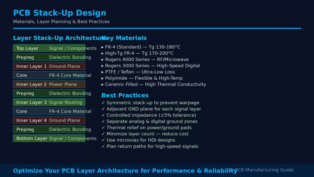
Two fundamental rules govern every stack-up: every signal layer must have an adjacent reference plane for a clean return path, and the stack-up must be symmetric about the board center to prevent warpage during manufacturing. Violating either rule guarantees problems downstream.
PCB Materials: Beyond Standard FR-4
Standard FR-4 (Tg 130–140°C, Dk ~4.2–4.5) works well for digital designs below 1 GHz. As frequencies climb, material properties — dielectric constant (Dk) and dissipation factor (Df) — directly control signal loss and impedance consistency.
| Material | Dk @ 10 GHz | Df @ 10 GHz | Tg (°C) | Best For |
|---|---|---|---|---|
| Standard FR-4 | 4.2–4.5 | 0.020 | 130–140 | General digital,<1 ghz=""> |
| Isola 370HR | ~3.9 | ~0.015 | 180 | Industrial, lead-free reflow |
| Megtron 6 | ~3.7 | ~0.004 | 185 | 25G–56G high-speed digital |
| Rogers RO4350B | 3.48 | 0.0037 | >280 | RF/microwave, mmWave |
| Megtron 7 | ~3.4 | ~0.002 | 200 | 56G–112G PAM4 |
| Tachyon 100G | ~3.0 | ~0.0014 | 200 | 112G+ ultra-low-loss |
Layer Count & Signal Layer Planning
Every signal layer must have an adjacent reference plane (ground or power) for a clean return path. A typical 6-layer high-speed stack-up arranges layers as:
L1: Top (Signal) — L2: Ground — L3: Inner Signal 1 — L4: Inner Signal 2 — L5: Power — L6: Bottom (Signal)
This arrangement gives every signal layer an adjacent reference plane. L1 references L2. L3 references L2 and L4. L4 references L3 and L5. L6 references L5. No signal layer is left without a nearby return path.
Symmetry is critical for preventing warpage. Copper distribution and material thicknesses must be mirror-symmetric about the board center. Asymmetric stack-ups — different copper weights or prepreg thicknesses on top vs bottom — are the leading cause of warpage in multilayer PCBs during reflow soldering.