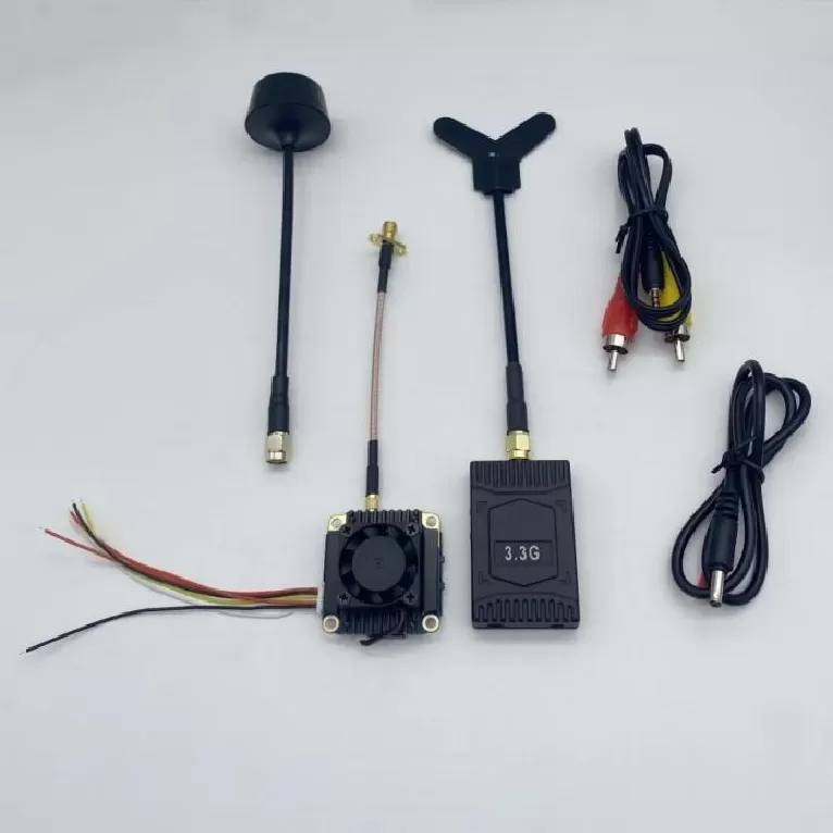
RF Front-End Board PCBA
RF Front End Board PCBA. RF PCBA, Power Amplifier, LNA, RF Front-End, Phased Array, Beamforming, Antenna Array, Frequency Synthesizer, Rogers PCB, VNA Test
Product Specifications
RF Front-End Board PCBA
Multi-Band Transmit/Receive Module for 4G/5G Wireless Infrastructure — 6–8 Layer Controlled-Impedance PCB
Product Overview
The RF front-end board PCBA integrates low-noise amplification on the receive path and linear power amplification on the transmit chain into a single high-reliability assembly. Engineered for 4G/5G macro base stations, small cells, and remote radio units (RRUs), this board covers 400 MHz to 6 GHz with a receiver noise figure below 2.5 dB and transmitter output power up to +33 dBm. The hybrid Rogers 4350B / FR-4 stack-up balances microwave dielectric performance with cost efficiency. Precision 50-ohm microstrip and grounded coplanar waveguide routing maintains VSWR below 1.5:1 across all RF ports. Advanced thermal management — including copper-coin inserts and dense thermal via farms under the PA stage — ensures reliable operation at case temperatures up to 85 °C. Every board ships with a full two-port S-parameter characterization report covering S11, S21, S12, and S22 from 10 MHz to 8 GHz.
Key Specifications
| Layer Count | 6–8 layers |
| Material | Rogers 4350B / FR-4 hybrid |
| Surface Finish | ENIG per IPC-4552 |
| Min. Trace/Space | 6/6 mil (RF), 4/4 mil (digital) |
| Impedance Control | 50 Ω ±10% single-ended |
| Frequency Range | 400 MHz – 6 GHz |
| Rx Noise Figure | < 2.5 dB (LNA input to IF output) |
| Tx Output Power | Up to +33 dBm (1 dB compression) |
PCBA Assembly Challenges
Assembling a hybrid RF/digital front-end board presents unique challenges where analog signal integrity and thermal management intersect. The LNA and PA MMIC devices are typically in QFN or laminate-based DFN packages that demand precise stencil design — stepped stencils with 4 mil thickness for fine-pitch RF pads and 5 mil for the exposed thermal paddle prevent both solder bridging and voiding. The thermal paddle void rate is held below 25% per IPC-7093 using optimized reflow profiles with a 150–180 °C soak zone and peak temperature of 240–245 °C. Coplanarity of the RF connector footprints (SMA, SMP, or Mini-SMP) relative to the board edge must be maintained within ±3 mil to avoid gaps that create impedance discontinuities. Discrete RF passives (0402 and 0201 chip inductors and capacitors) are placed with tight orientation control — inductors are oriented perpendicular to adjacent traces to minimize mutual coupling. Every assembled board undergoes automated optical inspection (AOI) on both sides, with additional 2D X-ray inspection of all QFN thermal paddles and BGA devices.
Test Strategy
Each RF front-end board follows a rigorous three-stage test sequence. Stage one — DC parametric test — verifies bias voltages, quiescent currents, and digital control interface functionality (SPI or MIPI RFFE) on every LNA and PA stage before RF power is applied. Stage two is a full two-port vector network analyzer sweep (10 MHz to 8 GHz) measuring S-parameters, with pass/fail masks defined per the board's specification document. Return loss limits are typically 15 dB minimum at all active RF ports; gain flatness is held within ±1 dB across the operating band. Stage three subjects the board to a 24-hour burn-in at +70 °C ambient while transmitting at rated power into a 50-ohm load, with periodic S-parameter re-measurement to detect any degradation. Boards destined for outdoor infrastructure also undergo a thermal cycling test (-40 °C to +85 °C, 100 cycles) on a sample basis per AEC-Q100 stress test guidelines.
PCB Manufacturing Difficulty
Fabricating a hybrid Rogers/FR-4 RF front-end board to IPC-6012 Class 3 RF/microwave standards demands careful process control. The dissimilar CTE values of the Rogers hydrocarbon-ceramic laminate and the FR-4 core — roughly 30 ppm/°C versus 14 ppm/°C in the z-axis — create registration challenges during lamination that are managed through symmetrical stack-up design and low-stress press cycles. The RF layer is typically placed on the outer layers with FR-4 inner layers for digital and power distribution, requiring precision depth-controlled laser drilling for blind vias that stop on the first inner copper layer. Plated through-hole vias in the PA region use filled-and-capped construction to prevent solder wicking during assembly and to provide a flat surface for the QFN thermal paddle. Impedance is verified on every production panel using TDR coupon measurement; coupons are placed at the panel edge and measured before depanelization. The final surface finish is ENIG per IPC-4552, with electroless nickel thickness controlled to 3–5 µm to avoid nickel-induced insertion loss at frequencies above 3 GHz. All finished boards receive 100% automated optical inspection per IPC-6012 Class 3 requirements before release to assembly.
More information