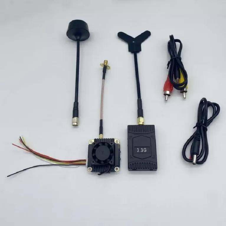
RF Combiner Board PCBA
RF Combiner Board PCBA. RF PCBA, Power Amplifier, LNA, RF Front-End, Phased Array, Beamforming, Antenna Array, Frequency Synthesizer, Rogers PCB, VNA Test,
Product Specifications
RF Combiner Board PCBA
High-Power Multi-Channel Gysel/Wilkinson Combiner for Broadcast and EMC Applications
Product Overview
The RF Combiner Board PCBA combines multiple high-power RF input channels into a single output with exceptionally low insertion loss, enabling power summation for broadcast transmitters, EMC test systems, and high-power jamming platforms. The board utilizes cascaded Wilkinson and Gysel combiner topologies with integrated high-power isolation resistors capable of dissipating imbalance power without catastrophic failure. Our thick-copper construction — 4 oz/ft² minimum on outer layers — handles continuous-wave power levels up to 500 watts combined, with thermal imaging used during design validation to confirm balanced heat distribution across all combining nodes. Each input port includes an integrated directional coupler for independent forward and reflected power monitoring; the combined output features a high-power termination port for safe load-pull and system-level testing. The symmetrical star-ground layout prevents ground loops that can cause spurious parametric oscillations in multi-amplifier combining configurations. All combiner boards undergo full-power burn-in testing with thermal cycling to validate long-term reliability under sustained high-power operation.
Key Specifications
| Frequency Range | 400 MHz – 6 GHz |
| Topology | Wilkinson / Gysel cascaded combiner |
| Combined CW Power | 500 W |
| Insertion Loss | <0.5 dB |
| Input Port Isolation | >20 dB |
| Output Return Loss | >18 dB |
| PCB Material | Rogers 5880 / Taconic RF-35 |
| Layer Count | 4–6 layers, thick copper (4 oz) |
PCBA Assembly Challenges
High-power RF combiner assembly demands thick-copper soldering process control far beyond standard SMT. The 4 oz/ft² copper planes act as massive heat sinks during reflow; profile optimization must extend soak time above 180°C to ensure the isolation resistors — typically flange-mount or high-power chip types — reach full liquidus without overheating adjacent low-temperature components. Isolation resistors dissipate imbalance power as heat and must be attached with high-thermal-conductivity solder (SnPb or AuSn) to a copper coin or direct-to-heatsink interface. Void inspection under these large power resistors via X-ray is mandatory — void rates above 10% create localized hotspots that reduce power handling by 30% or more. RF connector attachment for high-power interfaces (N-type, 7/16 DIN) requires controlled-torque soldering with post-attachment TDR verification to ensure the connector-to-microstrip transition maintains 50 Ω impedance and does not create a reflection hotspot at the board edge.
Test Strategy
Combiner board testing begins with low-power VNA characterization of all S-parameters from 10 MHz to 8 GHz to verify insertion loss, return loss, and port-to-port isolation. Following low-power verification, each board undergoes a staged high-power test: power is ramped in 50 W increments from a calibrated signal generator and amplifier chain while IR thermal imaging monitors the isolation resistors and combining nodes for hotspot formation. At full rated power (500 W CW), the board is soaked for a minimum of 30 minutes with continuous temperature monitoring at every resistor pad. Post-soak S-parameters are re-measured to detect any degradation from thermal stress. Intermodulation distortion is measured with a two-tone test at rated power to characterize the combiner's contribution to system-level linearity.
PCB Manufacturing Difficulty
Fabricating the bare PCB for a high-power combiner starts with thick-copper laminate processing. The 4 oz/ft² copper on Rogers 5880 requires specialized etching with controlled undercut compensation — standard etching produces trapezoidal traces that alter the designed impedance. The Gysel combiner topology requires precisely symmetric 180° electrical-length paths; any difference in dielectric thickness or copper roughness between the two halves creates a phase imbalance that reduces combining efficiency. High-power isolation resistors require large thermal land patterns with thermal via arrays directly under the component body; these vias must be filled and capped to prevent solder wicking during assembly. The ground plane must be continuous and low-inductance — any slot or split in the return path creates a radiating element at high power. Finished boards undergo thermal cycling qualification with thermal impedance measurement to validate the copper-to-dielectric bond integrity.
More information