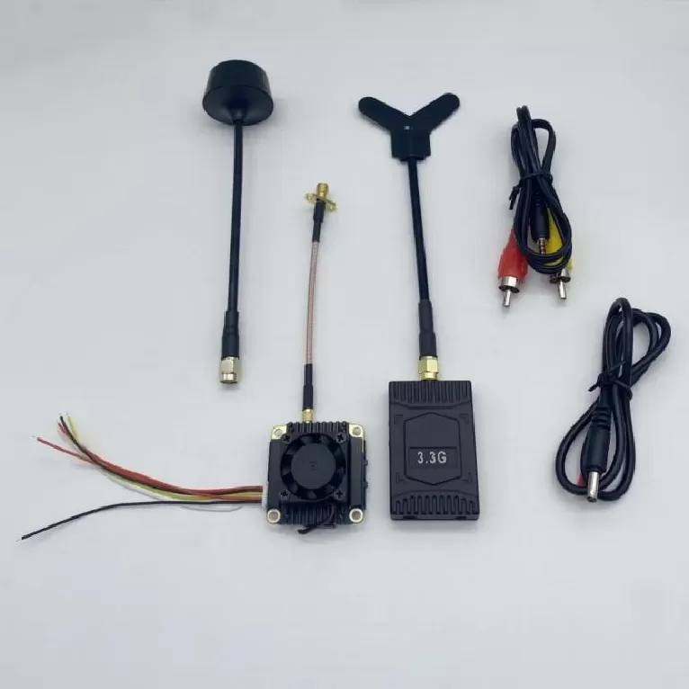
Phased Array Control Board PCBA
Phased Array Control Board PCBA. RF PCBA, Power Amplifier, LNA, RF Front-End, Phased Array, Beamforming, Antenna Array, Frequency Synthesizer, Rogers PCB,
Product Specifications
Phased Array Control Board PCBA
Electronically Steered Beam Control — 6-Bit Phase Resolution, <1 μs Beam Switching, 2–18 GHz
Product Overview
The Phased Array Control Board PCBA enables electronic beam steering across multi-octave frequency ranges from 2 to 18 GHz with 6-bit phase resolution and sub-microsecond beam switching. The board integrates digital phase shifters and attenuators on every channel, with a centralized beam-steering processor that computes element-level phase coefficients from commanded azimuth and elevation angles in real time. Multi-layer RF layout maintains consistent insertion phase through every channel using meandered transmission-line length equalization, achieving channel-to-channel phase tracking within ±3 degrees without per-element calibration. The control interface supports both pre-computed beam tables for rapid switching and real-time coefficient calculation for dynamic tracking applications. Onboard temperature sensors feed a compensation algorithm that corrects for phase-shifter thermal drift, maintaining beam accuracy from -40°C to +85°C. All channels are factory-characterized for phase and amplitude accuracy across frequency, temperature, and attenuator state. This PCBA serves as the core beam-steering engine for radar systems, SATCOM tracking antennas, and 5G mmWave phased arrays.
Key Specifications
| PCB Type | Phased Array Control Board |
| Frequency Range | 2–18 GHz |
| Phase Resolution | 1° (6-Bit) |
| Beam Switch Time | <1 μs |
| Material | Rogers 4003C / Megtron 6 |
| Layer Count | 10–16 layers, multi-channel |
PCBA Assembly Challenges
Assembling a phased array control board requires maintaining precise phase equalization across dozens of RF channels during the SMT process. The board employs large-footprint digital phase shifter and attenuator ICs — typically QFN or LGA packages — that must be placed with high coplanarity to ensure consistent ground-pad soldering. Any voiding under the ground paddle of a phase shifter introduces a parasitic inductance that shifts the insertion phase of that channel, directly degrading beam pointing accuracy. Void rates are held below 10% on all RF ground paddles, verified by X-ray inspection. The board's mixed-signal nature — combining sensitive RF paths with high-speed digital control buses — demands careful solder paste stencil design with stepped thickness in digital sections to prevent solder bridging on fine-pitch FPGA and memory components. The RF laminate (Rogers 4003C) requires a different reflow thermal profile than the digital section (Megtron 6), so the hybrid stackup is profiled with thermocouples on both sides to ensure all joints reach full liquidus without overheating the lower-Tg Rogers material. Post-reflow, every channel is tested for insertion phase continuity using a vector network analyzer.
Test Strategy
Each Phased Array Control Board undergoes a rigorous RF and digital test sequence. Flying probe testing verifies all bias, control, and power supply networks before RF testing begins. A multi-port vector network analyzer then characterizes every channel's insertion phase, insertion loss, and return loss across the full 2–18 GHz band with the phase shifters set to multiple states, generating a complete per-channel calibration map stored in onboard non-volatile memory. Beam switching speed is measured by toggling the beam-steering processor between two pre-stored beam tables and capturing the RF output envelope with a high-speed detector — any channel exceeding 1 μs of settling time is flagged. Thermal chamber testing cycles the board through -40°C to +85°C while the temperature compensation loop is active; phase drift at any channel must stay within ±2° of the temperature-corrected target. The beam-steering processor's computation engine is validated by commanding 10,000 random beam angles and comparing the computed coefficients against a golden reference model. Final system-level testing integrates the control board with the antenna aperture and measures far-field beam patterns to confirm pointing accuracy, sidelobe levels, and beamwidth across the full scan volume.
PCB Manufacturing Difficulty
Fabricating the bare PCB for a phased array control board demands exceptional phase consistency across all RF channels. The Rogers 4003C RF layers must maintain εr tolerance within ±0.02 across the entire panel — a single region with elevated dielectric constant would introduce several degrees of unwanted phase shift on the channels routed through that area. Transmission-line length equalization structures (meander lines) are modeled in 3D EM simulation to compensate for bend and corner effects, and every fabricated board is verified with TDR to confirm that equalized channel pairs match within ±1 ps. The hybrid laminate stackup bonds Rogers 4003C RF layers to Megtron 6 digital layers using low-flow prepreg with controlled resin content to prevent resin-starved regions that cause impedance discontinuities. Backdrilling removes via stubs on all high-frequency signal layers above 10 GHz to eliminate stub resonances, with stub length controlled to under 10 mil. Impedance coupons on every panel are tested with differential TDR to confirm 50 Ω single-ended and 100 Ω differential impedance within ±10%. 100% automated optical inspection is followed by netlist continuity testing before release to assembly.
More information