

RF, microwave and millimeter-wave devices form the fundamental building blocks of modern electronic information systems, wireless communications, radar detection, and cutting-edge quantum computing systems. These devices are responsible for signal generation, amplification, filtering, frequency mixing, transmission and reception. Their performance directly determines the bandwidth, signal-to-noise ratio and anti-interference capability of the entire high-frequency electronic system. According to medium-to-long-term forecasting models from research institutions, the global RF device market is expected to exceed USD 160 billion between 2030 and 2034 [Mordor Intelligence]
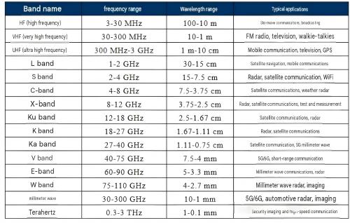
Table 1. RF and Microwave Frequency Band Classification and Applications
Market growth is mainly driven by 5G infrastructure deployment and rising integration levels of RF front-end modules in smartphones. As communication frequency bands extend to Sub-6 GHz and millimeter-wave, the quantity of filters, power amplifiers and RF switches deployed in a single terminal increases exponentially. Furthermore, the modernization of national defense has generated strong demand for high-voltage, high-power RF devices used in high-frequency electronic warfare systems, phased array radars and commercial low-earth-orbit satellite communications. In addition, the widespread adoption of 77 GHz millimeter-wave radars in autonomous vehicles has opened a vast incremental market for RF and microwave devices within automotive electronics.
This paper summarizes common active and passive RF & microwave devices and elaborates their core functions and operating principles. All cited products in this article are sourced from publicly available manufacturer datasheets.
1. Device Classification
RF and microwave devices can be categorized into passive devices and active devices based on whether external power supply is required.
1.1 Passive Devices
Passive devices implement linear transformation of microwave signals merely relying on their structural characteristics. They require no external DC bias, do not alter signal frequencies, and cannot generate new frequency components. Within RF systems, passive devices undertake functions including signal distribution, filtering, isolation, impedance matching, transmission and interconnection. Typical examples include filters, couplers, power dividers/combiners, etc.
1.1.1 Filters
Filters are classified into bandpass, lowpass, highpass and bandstop types. Their core function is to permit signals within a specific frequency range to pass through while suppressing (attenuating) signals at other frequencies. In communication systems, filters are applied for channel selection, spurious suppression and image frequency rejection; in radar systems, they separate transmit and receive frequencies.
Filters operate based on the frequency selectivity of reactive components (inductors and capacitors). As signals propagate through networks composed of inductors and capacitors, signals of different frequencies encounter distinct impedance, enabling frequency selection. An ideal filter features zero insertion loss within the passband and infinite attenuation in the stopband. The performance of practical filters involves trade-offs among multiple indicators: in-band insertion loss, stopband rejection, passband flatness, group delay and other parameters.
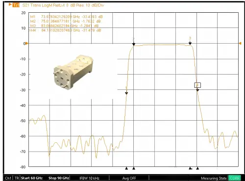
Figure 1. Millimeter Wave Product – E-Band Bandpass Filter, typical insertion loss: 1.5 dB, stopband rejection: 30 dB
1.1.2 Couplers
Directional couplers are four-port passive components that extract a portion of signal power from the main transmission line at a predefined coupling ratio with directivity: they couple forward-traveling signals while offering high isolation to reverse-traveling signals. Directional couplers are widely adopted for power monitoring, reflection measurement, signal sampling and automatic gain control.
The fundamental operating principle relies on electromagnetic field coupling between two or more parallel transmission lines. When electromagnetic waves propagate along the main line, partial energy is transferred to the coupled line via electric and magnetic coupling. By carefully designing the length and spacing of coupled structures, interference effects between forward and backward waves on the coupled line can be achieved to realize directional coupling.
.jpg)
Figure 2. Schematic Diagram and Product of Directional Coupler
A directional coupler generally consists of two parallel transmission lines: main line and coupled line. The four ports are defined as: Input Port (Port 1), Through Port (Port 2), Coupled Port (Port 3) and Isolated Port (Port 4). When a signal enters Port 1, most power exits from Port 2; a small fraction of energy is coupled to Port 3, while nearly no power appears at Port 4 (isolated).
1.1.3 Power Dividers / Combiners
A power divider is a passive component that splits input signal power into two or multiple output channels. When operated in reverse, it functions as a power combiner, aggregating multiple input signals into a single output. Power dividers are extensively used in feed networks of phased array radars, power combining and test & measurement applications.
The basic principle utilizes impedance transformation and power splitting characteristics of transmission lines to distribute input power evenly or proportionally among multiple output ports. Isolation resistors are typically installed between output ports to guarantee inter-port isolation. Common types include Wilkinson dividers, Gysel dividers and waveguide power dividers.
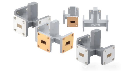
Figure 3. Multi-function Dual-Way Waveguide Power Divider [Pasternack]
1.1.4 Attenuators
Attenuators are passive devices that introduce a known amount of attenuation to RF signals. They are mainly used to adjust signal power levels, match system impedance, improve standing wave ratio and extend measurement dynamic range. Attenuators only reduce signal amplitude without modifying signal frequency or waveform. Attenuation is realized by resistive elements absorbing part of the signal power. According to circuit topology, attenuators can be categorized into resistive divider type, T-type, π-type, bridged-T type, etc. An ideal attenuator is purely resistive, featuring constant attenuation across the operating bandwidth and excellent input/output impedance matching.
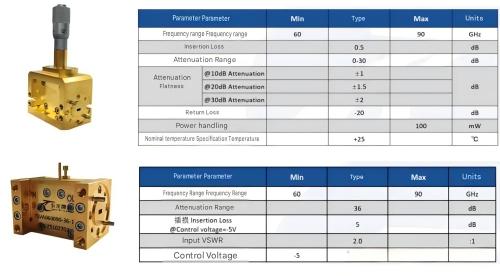
Figure 4. Waveguide Variable Attenuator and Waveguide Voltage-Controlled Attenuator [Tailai Microwave]
Conventional attenuators include fixed attenuators, digital step attenuators, voltage-controlled attenuators and step attenuators.
Fixed attenuators maintain constant attenuation; typical values include 1 dB, 3 dB, 6 dB, 10 dB, 20 dB, 30 dB, widely deployed where fixed attenuation is required.
Digital step attenuators adjust attenuation via digital control signals, usually cascaded with multiple attenuation bits. Each bit switches attenuation sections in or out using PIN diodes or FET switches. Common configurations: 4-bit (15 dB range), 5-bit (31 dB range), 6-bit (63 dB range), with minimum step sizes of 1 dB, 1 dB, 0.5 dB or 0.25 dB respectively.
Voltage-controlled attenuators achieve continuous attenuation tuning by bias-dependent resistance of PIN diodes or FETs. They support continuous adjustment but suffer inferior linearity and temperature stability.
Key performance metrics: attenuation value, attenuation accuracy, operating frequency range, attenuation flatness, VSWR, power handling capacity and switching speed.
1.1.5 Isolators / Circulators
Isolators and circulators are non-reciprocal passive devices based on ferrite materials. Their transmission characteristics differ for forward and reverse signal propagation, representing a small category of passive components that violate reciprocity theorem. The non-reciprocal behavior originates from the tensor permeability of ferrite under external DC bias magnetic field.
.jpg)
Figure 5. Operating Principle of Circulator and Isolator
Ferrite is ferromagnetic ceramic material. Under external DC bias magnetic field, its permeability exhibits tensor characteristics, meaning permeability varies with propagation direction. Electromagnetic waves traveling forward and backward through ferrite experience different interactions, generating non-reciprocal effects. This property enables the design of isolators (unidirectional transmission) and circulators.
1.1.6 Connectors and Adapters
RF connectors and cable assemblies are fundamental interconnection components in RF systems, transmitting RF signals between modules. Despite their seemingly simple structure, their performance directly affects overall signal quality. Especially for high-frequency and high-precision measurement systems, consistent impedance and low insertion loss across the operating band are mandatory.
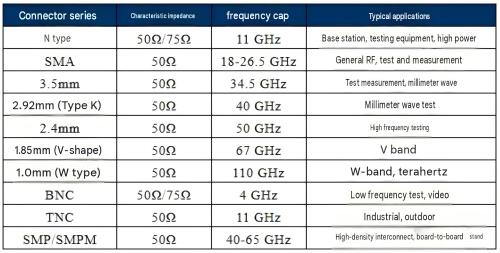
Table 2. RF Connector Series and Corresponding Frequency Ranges
1.1.7 Cable Assemblies
An RF cable assembly consists of RF cable and connectors mounted at both ends for signal interconnection between system modules. Classified by mechanical structure and electrical performance:
Semi-rigid cable: Outer conductor made of copper tube, outstanding shielding performance and stable phase characteristics, but limited flexibility. Suitable for fixed internal equipment wiring.
Semi-flexible cable: Outer conductor with tinned copper braid, moderate bending capability, performance close to semi-rigid cables.
Flexible cable: Multi-layer braided outer conductor, excellent bending property but relatively poor phase stability.
Low-loss cable: Adopts low-loss dielectric and optimized structure for low insertion loss, applicable for long-distance transmission.
Phase & amplitude stable cable: Maintains stable amplitude and phase under bending and temperature variation, targeting high-precision test and measurement.
Millimeter-wave cable: Supports ultra-high frequencies up to 110 GHz with specialized dielectric and structural design.
1.1.8 Terminations / Loads
Terminations are passive components connected at transmission line terminals to absorb residual power. Their input impedance matches the system characteristic impedance, so incident waves are fully absorbed without reflection. Terminations are widely used in test & measurement, system matching and power combining applications. They can be divided into low-power terminations (several watts) and high-power terminations (several kilowatts) by power rating, or coaxial terminations and waveguide terminations by form factor.
.webp)
Figure 6. Waveguide Termination [RFone]
1.1.9 Phase Shifters, DC Blocks, Bias Tees, Equalizers, Limiters, Detectors, Rotary Joints
Phase shifters adjust signal phase, playing vital roles in phased array radars, beamforming and test instrumentation. They are grouped into digital phase shifters and analog phase shifters by control mode. Digital phase shifters select discrete phase offsets via digital commands with high precision and repeatability; analog phase shifters offer continuous phase tuning through voltage control yet suffer inferior linearity.
.webp)
Figure 7. 0–180° WR-15 Waveguide Phase Shifter, 50 GHz – 75 GHz, with UG-385/U Round Cover Flange [Pasternack]
RF bias tee is a three-port passive component named after its T-shaped topology, comprising an RF I/O port, DC injection port and combined port. Its core function is to supply DC bias voltage/current to active circuits (amplifiers, mixers, etc.) without interfering with RF signal transmission. This architecture allows simultaneous transmission of RF signals and DC bias over a single transmission path, eliminating complex additional wiring.
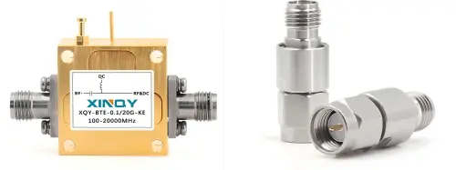
Figure 8. RF Bias Tee (Left) and DC Block (Right) [CoreChips]
A DC block is essentially a coaxial adapter equivalent to a high-pass filter with low cutoff frequency. It blocks DC and low-frequency signals while passing RF signals. It is commonly deployed to protect DC-sensitive RF components, isolate low-frequency interference during measurement, improve system SNR, suppress signal source modulation leakage and eliminate ground loops.
Equalizers feature frequency-dependent attenuation, typically presenting higher attenuation at lower frequencies and lower attenuation at higher frequencies. They compensate gain roll-off of amplifiers and cables to flatten the overall system frequency response.
Limiters serve as protective devices. Once input power exceeds a predefined threshold, output power is clamped within a safe level to prevent high-power signals from damaging sensitive downstream components such as low-noise amplifiers. They are generally constructed with PIN diodes or Schottky diodes.
2. Active Devices
Active devices require external DC power supply to operate. They are capable of amplifying, frequency-converting and switching signals, providing signal gain or generating new frequency components. Active devices constitute the core functional units for signal generation, amplification and transformation in RF systems. Main product categories: Amplifiers (low-noise amplifiers, power amplifiers, driver amplifiers, gain blocks); Mixers (up-conversion, down-conversion, harmonic mixers for frequency translation); Oscillators (VCO, DRO, crystal oscillators, frequency synthesizers for RF signal generation); RF switches (PIN diode switches, FET switches, MEMS switches for signal path routing); Frequency multipliers / dividers; Modulators / Demodulators (IQ modulators, vector modulators); MMICs (Monolithic Microwave Integrated Circuits integrating multiple functions on a single semiconductor chip).
2.1 Low Noise Amplifier (LNA)
The Low Noise Amplifier (LNA) is the first active component in receiver front-ends. Its primary function is amplifying weak received signals while introducing minimum additional noise to preserve receiver sensitivity. The noise performance of LNA directly determines the overall receiver noise figure, making it one of the most critical receiver components.
LNAs amplify faint RF signals utilizing transistor gain. To achieve low-noise performance, multiple design techniques are adopted: selecting low-noise transistors (GaAs pHEMT, InP HEMT); optimizing input matching network for minimum noise figure (noise matching); setting proper bias points to operate transistors within minimum noise region; adopting appropriate circuit topologies such as cascode configuration and multi-stage cascading.
Key performance indicators of LNAs:
Noise Figure: Quantifies noise introduced by the amplifier; lower value represents better performance. State-of-the-art LNAs achieve noise figure below 0.5 dB.
Gain: Ratio of output power to input power, typically ranging from 10 dB to 30 dB.
Gain Flatness: Gain fluctuation across the operating bandwidth.
Input / Output VSWR: Port matching performance.
Output P1dB: Output power at 1 dB gain compression point, characterizing linearity.
Third-Order Intercept Point (IP3): Metric for non-linear distortion.
Operating Frequency Range.
_142607.webp)
Figure 9. E-Band LNA [Mi-Wave]
This E-band low noise amplifier operates from 72 GHz to 82 GHz, covering key E-band spectrum for high-capacity wireless links, satellite communications and radar systems. It delivers typical small-signal gain of 30 dB (32 dB across full band), with typical noise figure of 4 dB and typical saturated output power of +14 dBm. As the first-stage active amplifier in millimeter-wave receive chains, the E-band LNA decisively governs the noise figure and dynamic range of the whole system. Heat sinks are recommended for prolonged saturated operation to enhance long-term reliability under harsh operating conditions.
2.2 Mixers
Mixers are three-port active or passive frequency-translation devices with three terminals: RF, LO (Local Oscillator) and IF (Intermediate Frequency). Based on the multiplication characteristic of non-linear elements, mixers multiply two signals of different frequencies to produce sum and difference frequency components, realizing up-conversion or down-conversion. Mixers are core components in communication transceivers, radars and test instruments.
The operating principle relies on the non-linear I-V characteristic of non-linear components (diodes, transistors) to multiply RF and LO signals and generate new frequency components. The output of an ideal mixer contains sum frequency (RF+LO) and difference frequency (RF−LO). Target frequency components are selected via subsequent filters.
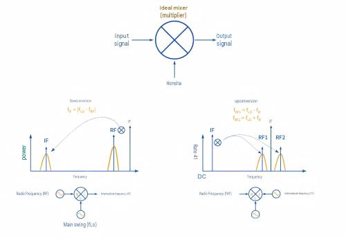
Figure 10. Simplified Schematic of RF Mixer and Idealized Down-Conversion & Up-Conversion Example
2.3 Frequency Multipliers
Frequency multipliers generate output signals at integer multiples of input frequency. Non-linear devices produce harmonic components, and target harmonics are extracted by filters. Multipliers are widely used for high-frequency signal generation, especially in millimeter-wave and terahertz bands where direct high-frequency oscillation is difficult to implement.
.webp)
Figure 11. Digital / Mixed-Signal Circuit Based on Phase-Locked Loop (PLL) Architecture
Taking the above circuit as an example, high-frequency signals are generated internally by the Voltage-Controlled Oscillator (VCO). The external reference signal only provides a timing benchmark. The feedback loop forces the VCO frequency to lock precisely at 100 times the reference frequency. The frequency multiplication process can be broken down into the following steps to illustrate signal flow until frequency lock is achieved:
Step 1. The external low-frequency reference signal (e.g., 10 kHz sine wave or narrow pulse) is AC-coupled via capacitor C1 (1 pF) into comparator LM339. At this stage, noisy or slowly rising analog signals are converted into standard square waves by LM339 and its peripheral resistors R2, R3, R4, R5 forming a Schmitt trigger. This square wave serves as the reference frequency baseline \(f_{in}\) of the whole system.
Step 2. The shaped reference signal \(f_{in}\) enters Pin 14 (phase detector input) of CD4046 PLL chip. Meanwhile, Pin 3 (comparison input) receives feedback signal from the return loop (upon startup, feedback frequency is extremely low or unstable). The internal phase detector of CD4046 continuously compares phase and frequency difference between the two input signals and outputs a pulse sequence containing error information from Pin 13.
Step 3. Error pulses from Pin 13 cannot be directly utilized. They pass through a low-pass filter constructed by R6, C3, C4 and R8, smoothing high-frequency pulses into steady DC control voltage \(V_{ctrl}\). If feedback frequency is lower than reference frequency, DC voltage rises; otherwise, voltage decreases. The smoothed \(V_{ctrl}\) is fed into Pin 9 (VCO control terminal) of CD4046. The internal VCO adjusts oscillation frequency in real time according to control voltage and outputs high-frequency square wave at Pin 4, namely the target output signal \(f_{out}\). The high-frequency signal \(f_{out}\) from Pin 4 is not fed directly back to the phase detector. Instead, it passes through two cascaded 74LS90 decimal counters. IC3 divides the high-frequency signal by 10, followed by IC4 dividing by another factor of 10. After two stages of frequency division, the signal fed back to Pin 3 of CD4046 becomes \(f_{out}/100\).
Step 4. Physical characteristics of PLL force continuous VCO adjustment until the two inputs of the phase detector achieve identical frequency. At steady state, the following equation holds: \(f_{in}=f_{out}/100\), i.e., \(f_{out}=100\times f_{in}\)
After generation, the target high-frequency signal enters the logic gate network on the right side. Inverter N1 inverts \(f_{out}\). NAND gate N2 receives inverted \(f_{out}\) and low-frequency square wave from the final stage of IC4. This configuration allows high-frequency clock pulses to pass only within a specific phase window of the low-frequency reference signal. The final signal passes through a 100 Ω matching resistor R9 and outputs for sampling or triggering of downstream circuits.
Conclusion
Additional topics including manufacturing processes, production workflows and supply chain management will not be elaborated here. From the perspective of industrial chain development, RF and microwave device technology is extending from microwave bands toward millimeter-wave and terahertz spectrum. Applications such as 5G millimeter-wave, 6G and automotive radar & imaging push operating frequencies higher continuously. Meanwhile, systems require ever wider bandwidth, imposing stricter wideband performance requirements on devices, and the industry exhibits a prominent trend of high integration. Driven by the evolution of 5G/6G, LEO satellite constellation deployment and advances in quantum computing, the RF and microwave device industry is entering an era with substantial structural technological dividends.





