

8-12 Layer Edge AI Module and Carrier Board PCB


Product Specifications
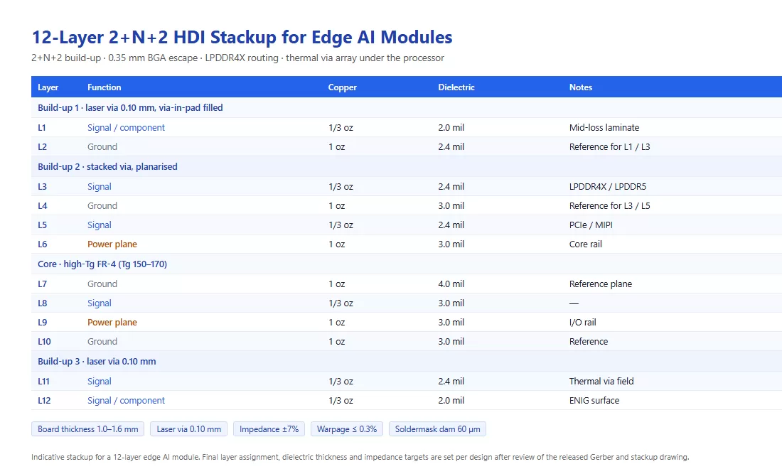
8 to 12-layer HDI for edge AI modules and carrier boards — 2+N+2 or 3+N+3 build-up, 0.35 mm BGA escape, LPDDR4X/5 routing, thermal via arrays and impedance control on a board that has to fit inside the enclosure.
Product Overview
Edge AI hardware splits into two boards that behave very differently from a server card. The module is the small board that carries the processor, memory and power stages; the carrier board is what turns that module into a product with Ethernet, USB, camera inputs, CAN and a power connector. Both run at 8 to 12 layers, both use HDI, and both are constrained by the enclosure rather than by the rack.
The power budget is 10 to 30 W rather than 500 W, so the electrical problem is not copper weight but routing density. A 0.35 to 0.5 mm pitch BGA with LPDDR4X or LPDDR5 at 4266 to 6400 MT/s needs short, length-matched, impedance-controlled traces on a board that is often 60 × 80 mm. Thermal management is by conduction to the case, which means thermal via arrays under the processor and a flat board that actually contacts the heatsink.
We build these as 8 to 12-layer 2+N+2 or 3+N+3 HDI, at 1.0 to 1.6 mm finished thickness, with 0.10 mm laser vias and 0.20 mm mechanical vias. Thin boards and fine-pitch BGA are the two things that decide yield on this class.
Key Specifications
| Parameter | Capability |
|---|---|
| Layer count | 8–12 layers, 2+N+2 or 3+N+3 HDI |
| Board thickness | 1.0–1.6 mm |
| Laser via | 0.10 mm, stacked or staggered, via-in-pad filled |
| Mechanical via | 0.20–0.25 mm |
| Minimum line / space | 3/3 mil inner, 4/4 mil outer |
| BGA pitch | 0.35 mm and above |
| Impedance control | ±7% differential |
| Memory routing | LPDDR4X / LPDDR5, length matched within 5 mil |
| Materials | Mid-loss or low-loss laminate, Tg 150–180 |
| Surface finish | ENIG standard, immersion silver on request |
| Warpage | ≤ 0.3% on 1.0 mm boards |
| Solder mask | LDI, 60 µm dam on 0.35 mm pitch |
| Panel utilization | Multiple-up with routed or V-cut separation |
Routing the Memory
LPDDR4X and LPDDR5 are the hardest part of an edge module. The bus is wide, the traces are short, and the skew budget is measured in a few mils. On a 0.4 mm pitch package the escape from the ball field consumes most of the available routing channels before the memory even starts.
Two things make it buildable. First, via-in-pad with filled and planarised vias, so the escape does not steal routing space on the layer below. Second, a stackup where the memory signals have an uninterrupted reference plane directly beneath them for the whole run. If the reference is split, the impedance changes mid-trace and the skew budget is gone regardless of how well the lengths are matched.
Thermal Path
An edge module conducts heat into the enclosure through the board and through a thermal pad on top of the processor. Both paths are manufactured features. Under the processor we place a thermal via array, typically 100 to 300 vias at 0.3 mm on a 0.8 to 1.0 mm grid, connected to a copper plane that spreads into the mounting area. The board then has to stay flat enough that the thermal pad actually makes contact: on a 1.0 mm board, 0.3% warp is the practical limit.
Manufacturing Challenges
Thin board, many laminations. A 1.0 mm 12-layer 3+N+3 build has very little core left after four build-up cycles. Press parameters have to avoid resin starvation in the thin core while still filling the via structures.
Via-in-pad without dimples. At 0.4 mm pitch, a 5 µm dimple is enough to trap solder and create a void under the ball. Fill and planarisation are verified by cross-section, and the surface is checked for copper thickness uniformity across the array.
Soldermask dams at 60 µm. Mask slivers that thin lift during reflow and bridge adjacent pads. LDI exposure with a tested dam width is the only reliable route at 0.35 mm pitch.
Panel utilisation versus routing density. Small boards are usually stepped multiple-up, which saves material but pushes registration tolerance across the panel. Registration is held per image, not per panel.
Mixed analogue and high-speed on one board. Camera MIPI lanes, USB 3, PCIe and switching power supplies share a small area. Plane partitioning and keep-out discipline decide whether the camera link works at full rate.
Inspection and Test
Flying-probe test on every net. Impedance coupons measured per panel. Via fill and mask dam verified by cross-section on first article. Warpage measured after reflow simulation. For assembled modules, 3D X-ray on the BGA field and functional test at temperature.
Applications
Edge AI gateways, industrial vision cameras, AI boxes for retail and access control, robotics controllers, drone payload computers, medical imaging front ends, and vehicle-mounted inference units.
Why Superb Automation
HDI at 0.35 mm pitch as a routine build. Via-in-pad fill, LDI mask and impedance coupons are part of the standard flow, not special requests.
Thin-board warpage control. Measured after reflow, on the actual board thickness, not on a coupon.
One supplier from bare board to assembled module. Fabrication and SMT in the same plant removes the handling risk between the two.
Component sourcing alongside fabrication. Twenty-five years of sourcing means the memory, PHY and power parts on the BOM are checked for availability before the build is scheduled.
Traceability to panel and lot. Lot codes map to material batch, drill program and test result.
Review of released files only. We do not design the board. We review the Gerber, stackup and impedance spec you release and quote from there.