

20-24 Layer AI Server Mainboard PCB


Product Specifications
20 to 24-layer mainboards for AI servers and accelerator host boards — back-drilled high-speed vias, 2–3 oz power planes, hybrid low-loss stackups and impedance held to ±7%.
Product Overview
An AI server mainboard is not a faster version of a general-purpose server board. It is a different board class. The processor package pulls several hundred amps at under one volt, the memory sits in HBM stacks rather than DIMM slots, and the links between processors, switches and NICs run at 56G NRZ or 112G PAM4. Every one of those requirements lands on the PCB as layer count, copper weight, dielectric loss and via geometry.
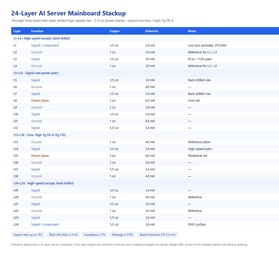
We build these boards at 20 to 24 layers, with a 4+12+4 or 6+12+6 HDI construction where the escape density demands it, and as straight through-hole builds with back-drilling where it does not. Power planes run 2 to 3 oz copper. High-speed through-vias are back-drilled to a residual stub of 4 mil or less. The stackup is hybrid: ultra-low-loss laminate on the layers that carry the high-speed pairs, high-Tg FR-4 on the plane layers where loss is irrelevant.
The manufacturing difficulty is concentrated in three places: keeping the power delivery network below a milliohm, keeping the stub short enough that 112G links open an eye, and keeping a 3 mm board flat enough for a 0.6 mm pitch BGA field after reflow.
Key Specifications
| Parameter | Capability |
|---|---|
| Layer count | 20–24 layers standard, up to 30 on request |
| Construction | Through-hole with back-drill, or 4+12+4 / 6+12+6 HDI |
| Residual stub after back-drill | ≤ 4 mil, depth tolerance ±2 mil |
| Minimum line / space | 3/3 mil inner, 4/4 mil outer |
| Copper weight | 2–3 oz power planes, 1 oz signal |
| Impedance control | ±7% differential, ±10% single-ended |
| Materials | Ultra-low-loss outer layers (Df 0.001–0.004), high-Tg FR-4 core (Tg 170–200) |
| Board thickness | 2.0–3.2 mm |
| Maximum board size | 620 × 580 mm |
| Aspect ratio | Up to 16:1 on mechanical vias |
| Surface finish | ENIG, immersion silver, ENEPIG on request |
| Warpage | ≤ 0.5% after reflow |
| Solder mask | LDI exposure, 75 µm dam |
Power Delivery
At 0.8 V core and 500 A, every milliohm counts. Ten milliohms of path resistance is an 0.5 V drop, which is more than the entire tolerance band. The board therefore has to deliver current with negligible DC resistance and low AC impedance up to roughly 100 MHz, and it has to do that without hot spots.
Three things make that work. First, copper weight: 2 to 3 oz on the power planes, with multiple parallel planes per rail rather than one thick plane. Second, via arrays: a 0.3 mm via carries roughly 2 to 3 A, so a 200 A rail needs 70 or more vias, distributed evenly rather than bunched under one corner of the package. Third, plane pair spacing: thin dielectric between power and ground gives the interplane capacitance that keeps high-frequency impedance down without adding discrete capacitors.
High-Speed Routing and Back-Drilling
A through-via on a 3 mm board leaves a stub. At 56G the stub is a nuisance; at 112G PAM4 an 8–10 mil stub puts a resonance inside the signal band and the link closes. Back-drilling removes the unused barrel from the bottom of the board, and the depth has to be controlled to ±2 mil to leave a stub short enough without cutting into the layer the signal actually uses.
Depth control is a tool-wear problem as much as a programming one. We track drill hits per tool, re-qualify the depth offset every 200 hits, and verify the first panel of each stack by cross-section. Production panels are checked by X-ray. Coupons on every panel are measured by TDR so the impedance result travels with the panel rather than with a separate test vehicle.
Manufacturing Challenges
Mixed dielectrics, one lamination cycle. Low-loss material and high-Tg FR-4 have different coefficients of thermal expansion and different resin flow. Laminating them in one press without voids or delamination at the interface requires a press profile built for the pair, not for either material alone.
Warpage on a 620 mm panel. Asymmetric copper and asymmetric build-up both bow the board. We balance copper per layer, keep the build-up symmetric, and stress-relieve after the final press. Warp is measured after reflow simulation, not after lamination, because that is when it matters.
Fine-pitch BGA escape on 24 layers. A 0.8 mm pitch field with 1,000+ balls needs six to eight escape tiers. If the escape is planned badly the board needs two more layers than it should, which is why we review the fan-out against the stackup before quoting rather than after the first panel fails.
Heavy copper etch compensation. A 3 oz plane etches differently from a 1 oz signal layer, and the same artwork compensation cannot serve both. Each copper weight gets its own etch compensation and its own measurement point.
Inspection and Test
Electrical test by flying probe on every net, with a fixture for volume. Impedance by TDR on per-panel coupons. Back-drill depth by cross-section on first article and X-ray in production. Via integrity by cross-section plus 500 thermal cycles from −40°C to 125°C on the qualification lot. Ionic contamination and solder mask adhesion are checked per lot.
Applications
AI training and inference servers, GPU and accelerator host boards, high-speed switch line cards, storage controllers with PCIe Gen 5 fan-out, HPC compute nodes, and network appliances carrying 112G SerDes.
Why Superb Automation
Board and bill of materials reviewed together. Twenty-five years in component sourcing means the material callouts on the stackup are checked against what is actually available before the first panel is scheduled.
Back-drill data per lot. Stub length and depth tolerance are reported, not assumed, with cross-section data on request.
Hybrid stackups as standard. Low-loss outside, high-Tg FR-4 inside, with a per-layer impedance model.
Traceability to panel, lot and press cycle. Lot codes map to material batch, drill program, plating run and test result.
Fabrication and assembly under one roof. The same plant that builds the 24-layer board can assemble and X-ray the finished unit.
Review of released files only. We do not design boards. We review the Gerber, stackup and impedance specification you release and quote from there.