

20-Layer 4-Stage HDI PCB for AI Accelerator Cards


Product Specifications
20-layer 4-stage HDI fabrication for AI accelerator cards — low-loss hybrid stackups, 3/3 mil routing, back-drilled vias, heavy-copper power planes and impedance control held to ±7%.
Product Overview
An AI accelerator card is the most demanding board in commercial electronics. A single package carries a server-class ASIC with 1,000+ ball pads, eight to twelve HBM stacks, 16 to 72 high-speed lanes and a power delivery network that has to move several hundred amps at well under one volt. Everything the board does — layer count, copper weight, dielectric choice, via structure, drilling tolerance — is set by those three problems: bandwidth, current and heat.
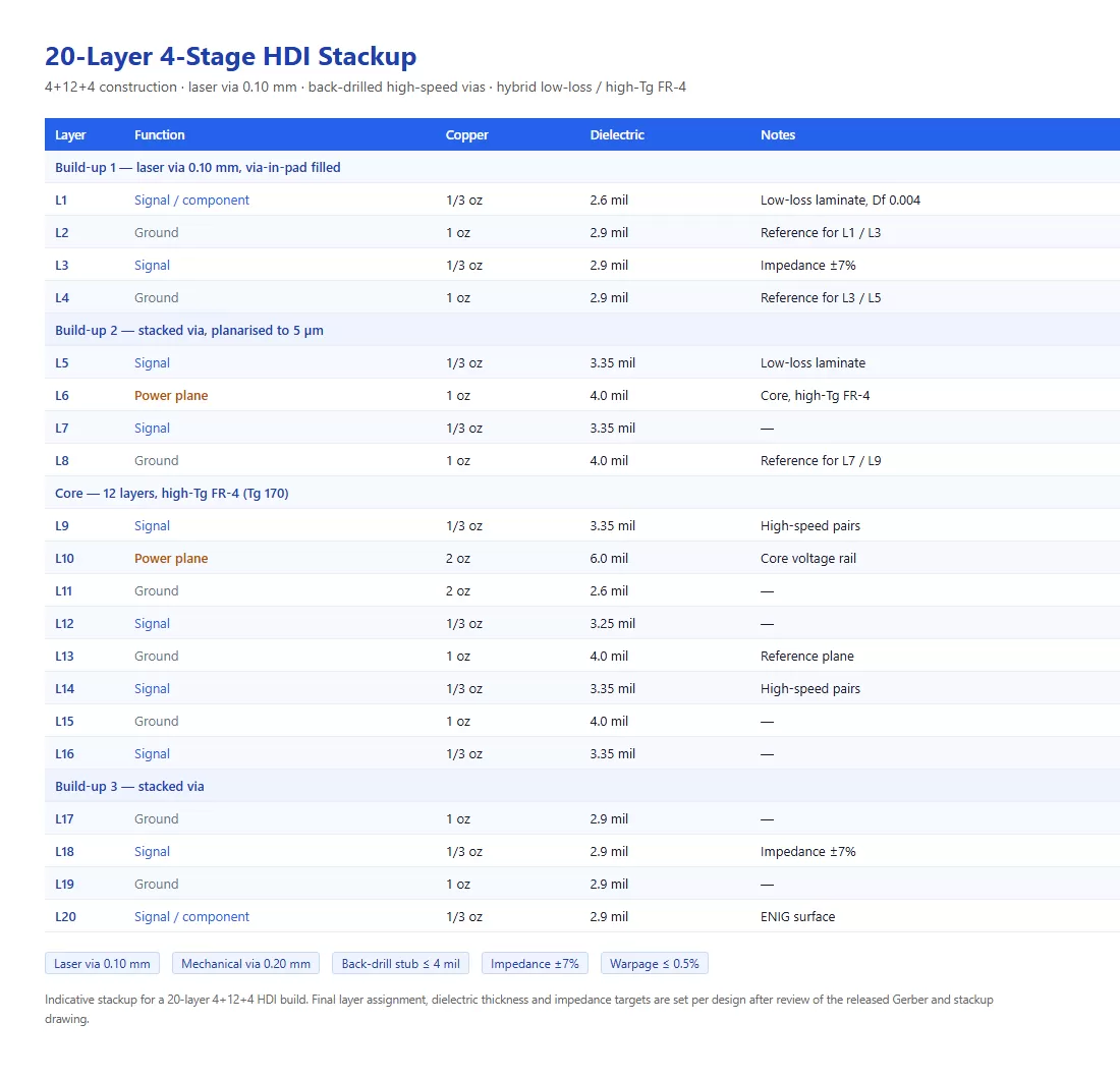
We fabricate these boards as 20-layer 4-stage HDI builds with a 4+12+4 construction. Four sequential build-up cycles per side give the escape density a fine-pitch ASIC needs, while the 12-layer core carries the power planes, ground reference and the low-speed control routing. Laser vias are 0.10 mm, mechanically drilled vias run down to 0.20 mm, and high-speed through-vias are back-drilled to a residual stub of 4 mil or less.
The stackup is hybrid rather than uniform. Ultra-low-loss material sits on the outer high-speed layers where 112G PAM4 and PCIe Gen 5/6 signals actually travel; high-Tg FR-4 fills the inner power and ground layers where loss does not matter. That combination keeps insertion loss inside the link budget without paying ultra-low-loss prices for 20 layers of laminate.
Key Specifications
| Parameter | Capability |
|---|---|
| Layer count | 20 layers (4+12+4), up to 30 layers on request |
| HDI structure | 4-stage build-up, stacked laser vias, via-in-pad filled and plated |
| Laser via | 0.10 mm finished, aspect ratio 0.8:1 |
| Mechanical via | 0.20–0.30 mm, back-drilled on high-speed nets |
| Residual stub after back-drill | ≤ 4 mil, depth tolerance ±2 mil |
| Minimum line / space | 3/3 mil (75/75 µm) on inner layers |
| Copper weight | 2–3 oz on power planes, 1 oz on signal layers |
| Impedance control | ±7% differential, ±10% single-ended |
| Materials | Ultra-low-loss (Df 0.001–0.004) outer layers, high-Tg FR-4 core (Tg 170–200) |
| Board thickness | 2.0–3.2 mm |
| Surface finish | ENIG or immersion silver; ENEPIG on request |
| Warpage | ≤ 0.5% after reflow, measured on 0.6 mm pitch BGA field |
| Solder mask | LDI exposure, 75 µm dam on 0.35 mm pitch |
Stackup Logic
Twenty layers is not a marketing number, it is the arithmetic of the package. Every high-speed signal layer needs an adjacent ground reference, so a routing tier costs two layers. A 1,000-ball ASIC at 0.8 mm pitch needs six to eight escape tiers before the traces reach the HBM field or the PCIe edge connector. Add four to eight power planes to spread several hundred amps, and the count lands at 20 to 24 before any margin is applied. Reducing layers forces either a larger board or more build-up cycles, and both cost more than the copper saved.
The 4-stage build-up exists for the same reason. Fan-out from a 0.8 mm ball field at 3/3 mil cannot be done on one or two laser layers without buried vias landing on top of each other. Stacked via-in-pad lets the first via land directly on the next, which is what makes the escape fit. That structure is also where most of the yield risk lives: every build-up cycle adds a lamination, an alignment step and a chance for resin voiding under the via.
Manufacturing Challenges
Four laminations, four alignment events. Each build-up cycle registers laser vias to the layer below. A 25 µm drift at stage three becomes a 100 µm error at the surface after four cycles. We use X-ray target drilling plus per-stage scaling compensation, and we measure registration on every panel rather than on a coupon.
Via fill without voids. Stacked vias require full copper fill, planarised to within 5 µm, or the next laser via lands on a dimple and cracks. Void-free fill is verified by cross-section at the start of every lot and by X-ray on production panels.
Back-drill depth on a 3 mm board. At 112G PAM4 an 8–10 mil stub puts a resonance inside the signal band. Controlling the remaining stub to 4 mil on a 3.2 mm board means depth accuracy better than ±2 mil, which is a routing and tool-wear problem as much as a drilling one. We track drill life per stack and re-qualify the depth offset every 200 hits.
Heavy copper and fine line on the same panel. Power planes at 3 oz need thick resist and longer etch; signal layers at 3/3 mil need thin resist and tight etch compensation. The two are plated and etched on different passes, and the panel is measured for both after lamination.
Warpage after four press cycles. Asymmetric copper distribution across a 20-layer hybrid stack bows the board during reflow, and a bowed board will not sit flat under a 0.6 mm pitch BGA. Copper balancing, symmetric build-up and a post-bake stress relief step keep warp under 0.5%.
Impedance across a hybrid dielectric. With low-loss material outside and FR-4 inside, the same trace width gives a different impedance depending on which layer it runs on. The impedance model is built per layer, not per design, and test coupons are placed on every panel for TDR verification.
Process Flow
Inner-layer imaging and AOI on the 12-layer core, then lamination of the core, drilling and plating of the mechanical vias, and back-drilling of the high-speed through-vias. The four build-up cycles follow: laser drill, desmear, via fill and planarisation, copper plating, imaging at 3/3 mil, AOI, then lamination of the next cycle. After the final build-up the board goes through solder mask by LDI, ENIG, electrical test, impedance coupon measurement, and a final AOI plus X-ray of the BGA field.
Inspection and Test
Flying-probe test covers opens and shorts on every net; a dedicated test fixture is available for volume. Impedance coupons are measured by TDR on each panel lot. Back-drill depth is checked by cross-section on the first panel of each stack and by X-ray on production. Via fill integrity is verified by cross-section and by thermal cycling, 500 cycles from −40°C to 125°C, on the qualification lot.
Applications
AI training accelerator cards, inference accelerator cards, HBM carrier boards, high-speed server mainboards, switch and NIC line cards carrying 112G SerDes, and FPGA-based compute cards in test and measurement equipment.
Why Superb Automation
Twenty-five years in components, ten-plus in board fabrication. The same team that sources the parts reviews the BOM and the stackup together, so material availability is known before the first panel is built.
Hybrid stackups as a standard option. Low-loss on the outside, high-Tg FR-4 inside, with the impedance model built per layer rather than per design.
Back-drill control measured, not claimed. Residual stub and depth tolerance are reported per lot, with cross-section data on request.
Traceability to panel and lot. Every board carries a lot code that maps to material batch, drill program, plating run and test result.
One supplier from bare board to assembled card. The same plant that fabricates the 20-layer HDI can assemble, X-ray and test the finished accelerator card, which removes the handling risk between fabricator and assembler.
Engineering feedback on released files only. We do not design the board. We review the Gerber, stackup and impedance spec you release, flag what will not build, and quote from there.